Quantcast
Channel: MD's Technical Sharing
Viewing all 63 articles
Browse latest View live

Using Prolific PL-2303HXA USB to TTL chipset on Windows 8

$
0
0
To avoid using the MAX232 level converter and a USB to serial adapter on my Mac Mini every time I needed to debug the PIC micro-controller via UART, I purchased a few USB to TTL modules from eBay, hoping that the PIC will simply appear as a serial port under Windows ready for use with any terminal program.

The module looks neat with output pins for GND, TX, RX, 3.3.V and 5.0V:


Although Windows 8 automatically installed the driver for the module, the installation was not successful with an error message "A device which does not exist was specified." shown inside Device Manager. The module works fine on Windows XP or Windows 7 and my other USB to RS232 adapter works fine under Windows 8.

Further research reveals that the module is using the PL-2303HXA chipset, which is not supported under Windows 8, as indicated on the manufacturer's driver download page:

Windows 8/8.1 are NOT supported in PL-2303HXA and PL-2303X (End-of-Life) chip versions.

What is so special about Windows 8 that prevents the PL-2303HXA/PL-2303X from working, while other variants in the PL2303 family work just fine? For all I know the only major difference is that Windows 8 requires the use of signed drivers, which is irrelevant since the Prolific driver is signed. In any case, the requirements of signed drivers on Windows 8 can be disabled by using the following BCDEDIT commands:
    bcdedit.exe -set loadoptions DISABLE_INTEGRITY_CHECKS
    bcdedit.exe -set TESTSIGNINGON


    With some research I found a suggestion here. Apparently it is a driver problem that prevents the PL-2303HXA chipset from working on Windows 8, and not a chipset problem. The solution is to use an older driver file (not the driver installer provided by Prolific) downloadable from here and choose to install the driver manually.  When prompted, click "Browse my computer for driver software", select the driver's INF file, choose "Let me pick from a list of device drivers on my computer", and select the Prolific driver version 3.3.2 which was created in 2008 (not the latest version):


    With this manual selection, the driver will be installed properly on Windows 8 and a new COM port will be added under the Ports (COM & LPT) section in Device Manager and can be used from any terminal program.

    But the question remains as to what prevents the latest driver of PL-2303HXA from working on Windows 8. My guess is that there are some problems with the latest driver and this particular chipset on Windows 8 and although the problems might be fixable, Prolific has decided to take this opportunity to end-of-life some older PL2303 models and force end users to upgrade to newer models.

    Interfacing HY28A LCD module with ILI9320 controller and XPT2046 resistive touch panel to PIC microcontroller

    $
    0
    0
    This is a cheap 320x240 2.8" TFT LCD module that uses the ILI9320 controller for the display and the XPT2046 controller for the resistive touch panel. I purchased the module over a year ago but only had the opportunity to try it out recently. The module has since been phased out by the manufacturer and replaced with the HY28B that uses the ILI9325C controller.

    Physical connections

    The module has two 20-pin connectors on each side:

    To my disappointment, the connectors on this module use 2mm pitch, and not the standard 2.54mm (0.1") pitch used by most hobbyist breadboards, sockets and connectors. I also tried to search eBay and could not find anything that might be useful, other than a few 6-pin connectors for the Zigbee module which also happens to use 2mm pitch, although I did find a photo here taken by someone who has jumper cables with small headers fitting the 2mm pin pitch of this module.

    This is the time when some creativity is needed. Luckily since many of the parallel communication pins on the two 20-pin connectors on both side of the module are not used, I am able to break some of the unused pins, leaving space for me to bend other pins and solder them to standard 2.54mm male connectors in order to fit a breadboard:


    Interfacing the LCD module

    Although the ILI9320 supports both parallel and serial communications, the HY28A module is configured to only use SPI. Using the example source code provided by the seller, I was quickly able to make this LCD show some text and graphics:


    One interesting thing to note about the ILI9320 is that it uses SPI mode 3, not SPI mode 0 like many other SPI devices. This Wikipedia article has a good description on the different clock polarities and phases used by each SPI mode. From a PIC point of view, this means setting the correct value for bit 8 (CKE - Clock Edge) and bit 6 (CKP - Clock Polarity) in the SPI1CON1/SPI2CON1 register according to the datasheet:

    bit 8 CKE: SPIx Clock Edge Select bit
    1= Serial output data changes on transition from active clock state to idle clock state (see bit 6)
    0= Serial output data changes on transition from Idle clock state to active clock state (see bit 6)

    bit 6 CKP:Clock Polarity Select bit
    1= Idle state for clock is a high level; active state is a low level
    0= Idle state for clock is a low level; active state is a high level

    For mode 0 (most SPI devices), you will need to set CKP = 0 and CKE = 1. For mode 3 (the ILI9320), CKP = 1 and CKE = 0.

    Interfacing the touch screen

    There are two variants of the HY28A module, one with the ADS7843 controller for the resistive touch screen and the other with the XPT2046 touch controller. The main difference is that the ADS7843 outputs analog voltages while the XPT2046 uses an SPI interface for the touch controller. My module uses the XPT2406 and has 5 pins:

    TP_IRQ - Interrupt Request. Low when a press is detected.
    TP_CS - SPI Chip Select
    TP_SDO - SPI Data Input
    TP_SDI - SPI Data Output
    TP_SCK - SPI Clock

    Like most other resistive touch controllers, the XPT2046 will return a raw coordinate value when a press is detected on the panel. For the coordinate to be useful, the code must convert it to a coordinate within the LCD resolution. To make things simple, the code can just look at the maximum and the minimum values that are returned when a press is detected on each corner of the panel and perform a linear conversion of the values to LCD coordinates:

    // height and width of LCD 
    #define MAX_X 240UL
    #define MAX_Y 320UL

    // coordinates of sample touch points at 4 corners of touch panel
    #define TOUCH_X0 255
    #define TOUCH_Y0 200
    #define TOUCH_X1 3968
    #define TOUCH_Y1 3775

    // calibration constants
    cal_x = (TOUCH_X1 - TOUCH_X0) / MAX_X;
    cal_y = (TOUCH_Y1 - TOUCH_Y0) / MAX_Y;

    // get the raw touch coordinates
    xpt2046GetAverageCoordinates(&tX, &tY, 5);

    // convert to LCD coordinates
    pX = (tX - TOUCH_X0) / cal_x;
    pY = (tY - TOUCH_Y0) / cal_y;

    Reading of the touch points can be done when TP_IRQ is low, indicating that a touch is detected. To reduce noises and achieve better accuracy, it will be better to perform several reads (5~10) for every press and calculate the average coordinate of the touched points. TP_CS must remain low when reading is performed, and set to high when reading is done. Coordinates reading must be stopped as soon as TP_IRQ is high, indicating that touch presses are no longer detected.

    I was quickly able to prototype a program that allows me to draw on this resistive touch panel:


    If you can't see it, the text reads "PPDS STMJ" and "BAHX MBA". The isolated drawing points are from the noises due to breadboard stray capacitance. A median filter can probably be used to remove these isolated points for better accuracy.

    I also tried to connect the points that are drawn and achieve a better output:


    The text reads "Hello ABC" in the first picture and "123" in the second picture. Ignoring the inappropriate connections between two adjacent characters (due to the inability to detect when the stylus is released from the screen to stop connecting points), the other problem is the zig-zag and not smooth shape of the drawing. This is probably because of the slow speed of the PIC24. At 16MHz SPI speed and 32MHz clock speed on my PIC24FJ64GA002, some precious time is wasted communicating with the touch controller, calculating the touched coordinates and plotting them. During this time, other points drawn by the user were lost and not plotted on the screen.

    As it takes considerable time to read the touch points and plot them, it is not possible to migrate the entire process into an interrupt to increase touch sensitivity as an interrupt routine also needs to finish executing as fast as possible. The only solution for a smooth drawing would be a much faster clock speed, or perhaps to use Direct Memory Accessing (DMA), supported by this PIC. However, at this moment I do not yet have the time to explore either option.

    Sample code download

    C30 code for the ILI9320
    C30 code for the XPT2046

    Codes for both the LCD and the touch panel make use of my custom SPI library for the PIC24FJ64GA002 to facilitate SPI communication. Before working with the LCD or the touch screen, you will need to initialize the SPI modules using the spiInit method from my SPI library as shown below:

    spiInit(1, 0b00011011, 0); // SPI Module 1 for Touch Screen, secondary prescale 2:1, primary prescale 1:1, SPI mode 0
    spiInit(2, 0b00011011, 3); // SPI Module 2 for LCD, secondary prescale 2:1, primary prescale 1:1, SPI mode 3

    Assuming that the PIC is running at 32MHz, the above code will set the SPI clock at 16MHz, fast enough for many purposes.

    Exploring Tektronix TDS 340 100MHz digital storage oscilloscope

    $
    0
    0
    Out of curiosity, I purchased a Tektronix TDS 340 100 MHz 2-channel digital storage oscilloscope from eBay. It passes self-test at startup and is able to show the 1kHz square wave calibration signal on both channels nicely:

    The first thing on this oscilloscope that captures my attention was the faceplate on the top right of the device. This is for the 1.44MB 3.5" floppy disk drive, featured in the TDS 340A, which probably shares the same enclosure design with the TDS 340. However, don't expect to remove the faceplate and connect a PC floppy drive, or even a floppy drive from another TDS 340A, into the TDS 340 because the floppy drive interface board is not present on the TDS 340.

    This oscilloscope supports up to 500MS/s sampling rate and has a memory of 1000 samples. Two internal memory slots, REF1 and REF2, are available for user to store waveform data for manipulation. It also supports external trigger, delayed timebase and some math operations on the input signal. Overall, it is good enough for most of my hobbyist micro-controller and analog projects.

    The only thing I do not like about this oscilloscope is the AUTOSET feature. Among other things, it will set the acquisition mode back to 16-point average, instead of sampling. This causes a slower signal display, which is apparent when signal is removed from the probe - it will take a few seconds for the trace to update completely as the data points from the previous signal are still in the oscilloscope memory.

    Fast Fourier Transform (FFT)

    You can also perform FFT on the input signal and see the frequency components using the MATH menu. The following is the FFT of the 1kHz calibration signal:


    Using the CURSOR menu, I am able to measure the first FFT peak of 1kHz, the fundamental frequency of the signal, and the harmonics frequencies. A good revision on FFT and signal theory which I learned back in my university days. :)

    As I noticed, the FFT output on this oscilloscope is pretty noisy, compared to the smoother FFT waveform generated by the Rigol DS1052E of the same 1kHz signal:


    Why is this the case? I leave this as an exercise for the reader. A hint is that the TDS 340 supports only average acquisition mode when FFT is used whereas the Rigol supports all acquisition modes (normal, average, peak detection) even with FFT enabled and has other menus to configure FFT window and sampling options.

    Installing the Option 14 interface card

    To be able to transfer the captured signal data to a computer for manipulation, I decided to purchase an Option 14 interface card from eBay and install it in the oscilloscope. This card features a parallel printer port, a male DB9 RS-232 serial port, a 9-pin female VGA port and a GPIB interface port:


    The card has a 50-pin IDC male port used for communication with the oscilloscope and a 6-pin cable for video output. Although Option 14 boards can be safely interchanged between TDS340A, TDS340 and other similar models, some cards, especially those meant for the TDS 340A and later generations, also have another power cable that must be connected to a dedicated socket in the oscilloscope power supply. This is to provide power for some supported portable printers as seen in the photo below (notice the power socket):


    If these boards are used in the TDS 340, the printer power supply cable should be left unconnected.

    When purchasing a used Option 14 card, make sure it comes with the necessary cables. Mine came with the video cable but not the 50-pin cable. Luckily my 50-pin SCSI single-drive IDC female-to-female cable worked just fine. If you have to use a SCSI cable like what I did, make sure that the cable is single-drive and has no built-in terminators or other circuits to set the SCSI device ID, which may interfere with the communication and cause unexpected problems. The cable will need to be at least 40cm long to connect to the mainboard.

    The edges of the GPIB port make it impossible to fit the card into the back of the oscilloscope that has horizontal metal bars. I need to cut the bars for the card to fit in:


    Although the IDC cable is keyed to prevent wrong insertion, the video cable is not. However, during my experiment, inserting the video cable in the wrong direction will simply stop the VGA port from outputting video without any other long-term effects - all I need to do is reinserting the cable correctly. Obviously, don't leave the cable incorrectly connected for extended period. The pictures below show how to correctly connect the video cable (notice the colors of the individual wires) and the IDC cable:


    VGA output from the Option 14 card

    After installation, reassemble the oscilloscope, power it on to make sure that it still passes self-test and press the HARD COPY button. If the card is detected, after a short while, you will see an error message "Hardcopy device not responding" instead of the usual information on how to install the hard copy interface:


    The next test is to see if the VGA port on the card is working well. Page 144 of the TDS 340 technical reference provides the pinout for the DB9 VGA port:

    This is the pinout for the more common 15-pin VGA port, used in most modern devices:


    I made an adapter with the following pin configuration to be able to feed it into a standard VGA monitor:
    • Pin 2 of Option 14 DB9 VGA port (Video) connected to pin 2 (Green video) of VGA connector.
    • Pin 1 (Red video) and pin 3 (blue video) of VGA connector must be grounded.
    • Pin 4 of DB9 VGA port (Horizontal Sync) connected to pin 13 of VGA connector.
    • Pin 5 of DB9 VGA port (Vertical Sync) connected to pin 14 of VGA connector.
    • Pin 6,7,8 of DB9 VGA port (Ground) connected to pin 5,6,7,8,10 of VGA connector.
    • Pin 11 (Monitor ID) of VGA connector must be grounded. This indicates a 640x480 low-resolution VGA output and reduces the need to send monitor information via I2C using the DDC SDA and DDC SCL pins.   
    This is the back of the oscilloscope with the Option 14 card installed and the VGA adapter connected:


    This is the VGA output on my 24-inch LCD monitor:


    Using the hard-copy feature

    With the Option 14 card installed, the oscilloscope supports sending a capture of the current oscilloscope display, known as hard copy, via any of the following methods:
    • Printing to common parallel/serial printers at the time
    • Sending raw image data via RS232 or GPIB
    As I do not have any of the supported printers or a device with a GPIB port, I can only test the hard copy feature via RS232. To try this, press the UTILITY button, choose System I/O from the bottom left menu, select RS-232 for Hcp Port and configure the proper serial settings in the RS-232 bottom menu. Disable "Hard-flagging" (refers to serial hand shaking via the dedicated lines) and "Soft-flagging" (refers to XON/XOFF software handshaking) as they are just going to cause problems.

    You can configure the output file format in the Hcp Format menu. The TDS 340 supports BMP, TIFF, PCX, PostScript (PS) and Interleaf image formats. Except for Interleaf which I couldn't find a viewer for, the rest of the file formats are readable on the PC by most modern document viewers.

    You will need a cross-over serial cable and a computer with a serial port to receive the hard copy data. A USB to serial converter should work just fine as the data transmission does not rely much on the latency of the serial connection or the exact output voltage.

    In my tests, I use Realterm to capture the serial data sent once the HARDCOPY button is pressed. At the maximum RS232 speed of 19200bps on the TDS 340 (the TDS 340A supports a higher speed of 38400bps), it takes almost 20 seconds to transfer the 37.5KB 640x480 monochrome bitmap image produced by the oscilloscope. The image size reduces to approximately 18KB if PCX is used. The following is a monochrome bitmap produced by the hardcopy feature, optimized for printing:


    To avoid having to rotate the image on your computer, the Hcp Layout option should be set to Portrait.

    Downloads for TDS 340A, TDS 360 & TDS 380 oscilloscopes:

    User Manual
    Technical Reference
    Programmer Manual
    Service Manual 

    See also:

    Programming the Tektronix TDS 340 100MHz digital storage oscilloscope
    Calibration and acquisition problems on Tektronix TDS 340 oscilloscope

    Programming the Tektronix TDS 340 100MHz digital storage oscilloscope

    $
    0
    0
    In my previous article I provided some information on the Tektronix TDS 340 100 MHz digital storage oscilloscope and instructions on how to install the Option 14 card to get VGA output and support for hard copy. This article will provide some further information on interfacing the oscilloscope with a computer using the RS-232 port to retrieve raw signal data and share some of my interesting findings.

    Using the serial interface

    The oscilloscope serial port must first be configured inside the Utility>System I/O menu and a cross-over serial cable is needed to connect the oscilloscope to the PC. It is best to turn off both hardware and software handshaking as they are not going to help much and will just cause problems. The recommended serial settings are 19200bps, 8 data bits, no parity, 1 stop bit and carriage-return (CR) line ending.

    To check if the connection is working, use a terminal software such as Tera Term Web 3.1, configure it to echo characters locally with CR line ending, and type ID? followed by the ENTER key to ask the oscilloscope to return its identifier string, which should look like:

    TEK/TDS340,CF:91.1CT,FV:v1.00
       
    Commands are case-insensitive and multiple commands or responses are separated by a line ending character (CR, LF or CR/LF as configured). Commands ending with a question mark (?) are queries and a response from the oscilloscope is to be expected. Commands not ending with a question mark will simply be executed by the oscilloscope with no value returned. To check if there are any errors during command execution, use the following:

    *ESR?   // Show the value of the Event Status Register
    ALLE?   // Return the error log, which will show any errors with the commands previously sent

    The following command set, extracted from the programmer manual, measures the frequency of the input signal at channel 1:

    MEASU:IMM:SOURCE CH1  // Set measurement source to Channel 1
    MEASU:IMM:TYPE FREQ   // Measure the signal frequency
    MEASU:IMM:VAL?        // Get the measurement value

    If the probe of channel 1 is connected to the 1kHz calibration point in front of the oscilloscope, the above command set would return a value of approximately 1.0000E3, indicating a frequency of 1000Hz.

    Retrieving raw waveform data

    Command CURV? is used to ask the oscilloscope for the raw measurement data of the waveform being displayed. The following code will return all 1000 data points in the oscilloscope data acquisition memory:

    DAT:SOU CH1     // Measurement source to Channel 1
    DAT:ENC ASCI    // ASCII format
    DAT:WID 2       // 2 bytes data width
    DAT:STAR 1      // first data point
    DAT:STOP 1000   // last data point (1000th)           
    CURV?           // get waveform data


    The response will be a set of comma separated integers:

    22784,23040,-6656,[.....],-6656,23040

    The range of each returned integer value is –128 to 127 when DAT:WID is 1. Zero is center screen. The range is –32768 to 32767 when DAT:WID is 2. The upper limit is one division above the top of the screen and the lower limit is one division below the bottom of the screen.

    To properly interpret the data, it will be useful to know the oscilloscope settings via the WFMPR? command, which will return the following:

    2;16;ASC;RP;MSB;"Ch1, DC coupling, 2.0E0 V/div, 5.0E-4 s/div, 1000 points, Sample mode";1000;Y;"s";1.0E-5;500;"Volts";3.125E-4;1.28E4;0.0E0

    Among the returned values, the voltage per division, the time per division and sampling rate parameters (highlighted) will be needed to accurately analyze the returned data.

    Taking a screenshot of the oscilloscope

    A screenshot of the oscilloscope display can be captured progammatically using the following commands:

    HARDC ABO           // abort any existing hard copy
    HARDC:FORM BMP      // set hard copy format to bitmap
    HARDC:PORT RS232    // hard copy port to RS232
    HARDC STAR          // start hard copy


    The image data will be sent via the serial link. Unlike other commands, there is no end of file marker for the HARDC STAR command. To identify when to stop receiving data programmatically, one way is to count the number of bytes received and compare with the expected value. As the file size could vary depending on the hard copy output settings, an easier way is to assume that the hard copy operation has ended if no data is received after a certain period, e.g. 2 seconds.

    Custom PC interface software

    With some free time I made a .NET application that allows the user to retrieve the frequency measurements, waveform data as well as taking a screenshot of the oscilloscope:


    To use the application, first configure the serial port settings (port number, baud rate) and click on Open Port to initialize the serial interface. The Activity Log text box shows the commands sent and responses received. The Screenshot button will request for a screenshot from the oscilloscope and show it in the application. If option Show original color is checked, the application will convert the black-on-white image returned by the TDS340 to green-on-black, to make it look more like a real screenshot.The Event Log button will show all error messages currently in the oscilloscope event log.

    The application is using the SerialPort component of the .NET framework.  It assumes that both hardware and software handshaking is disabled in the oscilloscope serial settings. Interestingly, even with handshaking disabled, the DTR (Data Terminal Ready) and RTS (Ready To Send) lines must be on, otherwise the oscilloscope will not respond to the data sent. This is done using the following C# code:

    SerialPort1.Handshake = false;
    SerialPort1.DtrEnable = true;
    SerialPort1.RtsEnable = true;

    Due to the asynchronous nature of the DataReceived event of the .NET SerialPort component and the limited time that I have, I did not attempt to make the application wait for all data to be received before enabling the action buttons. For this reason, you will need to wait for a while and check the activity log after pressing any button to make sure that the command has finished executing before peforming the next action, otherwise the application behavior may be unexpected.

    Download the PC application here

    The Visual Studio 2012 source code is included in the download package. Microsoft .NET Framework 2.0 (which is installed by default on Windows 7 or later) is required. The executable can be found in the bin folder.

    Downloads for TDS 340A, TDS 360 & TDS 380 oscilloscopes:

    User Manual
    Technical Reference
    Programmer Manual
    Service Manual 

    See also:
     
    Exploring Tektronix TDS 340 100MHz digital storage oscilloscope 
    Calibration and acquisition problems on Tektronix TDS 340 oscilloscope 

    Calibration and acquisition problems on Tektronix TDS 340 oscilloscope

    $
    0
    0
    During one of my experiments with the TDS 340 oscilloscope made by Tektronix, I suddenly noticed that the AUTOSET button does not set the correct parameters for most signals, including the 1kHz calibration signal. Although it worked fine for a long time, the button now sets the oscilloscope to 5V/div, 25ms/div with wrong trigger settings, obviously not optimal to display a 1kHz square wave:


    Thinking that the oscilloscope is out of calibration, I ran a self-calibration using the UTILITY menu, only to find out that things have gotten worse. The calibration process failed after 4 minutes and the oscilloscope reported problems upon power on:


    WIth all input signals removed, I ran a diagnostics test from the UTILITY menu and sure enough, acquisition and calibration errors were reported:


    The error log provided some more details - the calibration issues may have been due to the acquisition problems affecting certain tests during the calibration process. Problems with trigger and signal path of Channel 1 (error codes diagAcq_ch1Trigger, diagAcq_ch1SigPath and diagAcq_holdoff) were reported:


    No errors were reported with channel 2. Are these errors related to my autoset problems? To answer this,  I performed a simple test by turning of channel 1 waveform display, feeding a signal to channel 2 and press AUTOSET. Surprisingly, autoset worked just fine and selected the correct settings to display a stable waveform on channel 2:


    So some problems with channel 1 prevented the oscilloscope from detecting the correct settings in autoset mode. Determined to find the issue, I opened up the oscilloscope and located the acquisition board:


    To my disappointment, unlike other Tektronix oscilloscope models, this acquisition board is also the mainboard of the oscilloscope and is very compact with mostly surface-mounted components. There are no through-hole electrolytic capacitors on the board which may cause problem as the capacitors become dry and fail with time. Although I did find some posts here and here referring to a problem similar to mine, my limited time and the nature of the problem prevented me from putting in more efforts to fix the issue. Except for the autoset feature, the oscilloscope still seems to be stable and works well even at high frequencies. I decided to live with the issue and manually select the correct settings for each input signal until some other more serious problems occur.

    See also:

    Programming the Tektronix TDS 340 100MHz digital storage oscilloscope
    Exploring Tektronix TDS 340 100MHz digital storage oscilloscope

    Capturing data from a Tektronix 1230 logic analyzer by emulating a parallel port printer

    $
    0
    0
    As a fan of vintage measurement equipments such as oscilloscopes and logic analyzers, I sometimes encounter the problem of extracting data from these machines onto external devices for storage or further analysis. While some of these old devices allow saving data to floppy drives or feature serial or GPIO ports and associated protocols to communicate with PCs or other devices in order to extract measurement data or capture screenshots, many other devices only support printing data in hard-copy to parallel or serial printers, which are hard to find nowadays. Recently while working with an old Tektronix 1230 logic analyzer, I spent some time tackling this problem and this article will share some of the achievements I have made and other interesting findings.

    The device

    I acquired this Tektronix 1230 from eBay, a vintage logic analyzer in the 1980s but still useful for troubleshooting old 8-bit designs. The following photos show the logic analyzer, with a Centronics parallel port and a DB25 RS-232 port at the back:


    A word of warning here for those intending to collect this vintage equipment. Make sure that your 1230 comes with probes (also known as pods) - you will want the P6444 or P6443 16-channel probe. Probes can be hard or expensive to purchase separately. It should also preferably come with RS-232 or Centronics ports for data output.

    The challenge: transferring captured data

    My challenge came when I wanted to export the capture data from this logic analyzer. Although it has a RS-232 port supporting up to 9600bps, communication with the device requires the S43R101 1230/PC application software made by Tektronix. During my research, a serial protocol for custom-made application to work with the logic analyzer via the serial port seems to be available and documented in the manual. Unfortunately, I could never locate a copy of the manual or the application software for this device available for download, apart from this information sheet. There is, however, plenty of information on the Internet for the Tektronix 1240, a later model. Extracting data via the serial port therefore seems infeasible.

    The only other way is to print data via the Centronics parallel port. Although I do not have any parallel port printer nowadays, a thought suddenly came across my mind that I might be able to program a PIC microcontroller to act as a parallel port printer and save the output data to an SD-card for further actions. Well, as they say, thoughts are dangerous and within minutes I found myself soldering wires to a DB25 parallel connector and interface it to a PIC24FJ64GA002 microcontroller.

    The Centronics printer protocol

    This is the Centronics parallel port pinout:
    Attempting this project requires knowledge of the Centronics protocol used for communication with parallel port printers, described in details on this page. For our purposes of emulating the parallel port printer. we will only need to care about the ACK, STROBE, BUSY signals and the D0-D7 lines. In the simpler polled mode of the Centronics protocol on a standard parallel port, the host (referring to the logic analyzer in our case) would send a pulse on the STROBE line to indicate it's going to send printing data. After that, the printer (or the PIC microcontroller in our scenario) will need to set the BUSY line high while at the same time reading for an input byte from the D0-D7 lines. When processing is completed, the printer will send a pulse on the ACK line and set the BUSY line low, indicating it is ready for the next command. The process is illustrated in the following timing diagram:


    To indicate that the emulated printer is available and ready for printing, Paper End (pin 12) should be connected to GND while Error (pin 15) and Select (pin 13) should be connected to 5V.

    Result: a PIC-based virtual parallel port printer

    Using the ST7735 1.8" color LCD (see my previous post) and the Microchip SD card library, I was able to build a working virtual printer. The device would listen for data being sent from the parallel port and save the print job to a .PRN file on the SD card. The following photos show the printer in action:


    The 1.8" LCD shows the SD card volume label, file system type, total capacity and free space. The name of the file containing the last print job is also displayed on the LCD. 

    As the PIC does not understand the data being sent and simply writes the data received on the SD card, there is an issue of telling when the print job finishes in order to start a new output file. On a real printer, the printer would detect the paper feed command and eject the page when a page has finished printing. In my case, I have chosen a simplified approach - assume that printing has ended and close the output file if no data is received after a certain period, e.g. 5 seconds. This would be sufficient for most purposes.

    Reading the printer output

    This emulated printer should work well with any application expecting a generic parallel port printer. It may not work if the application is expecting a specific modern parallel port printer model, in which case customized identification data might be sent via the parallel port in ECP or EPP mode to communicate with the application. For a simple test, executing the DOS command DIR > LPT1 or DIR > PRN with the printer connected to the LPT1 port should result in a .PRN file containing the list of files and sub-directories in the current directory being written to the SD card.

    On the Tektronix 1230, printing can be done by double-pressing the NOTES key (to print a screen capture) or by pressing the D key (to print memory contents), as described in the help screen:


    While pressing D will print the memory contents in text format, double-pressing the NOTES key (supported only on Epson-compatible printer) will print a graphics representation of the current screen. Although printing of memory contents will not hang the logic analyzer and the printer status will be displayed as "Printing", the logic analyzer will stop responding while the screen is being printed.  Also during my experiment, if the status lines on the Centronics parallel port report conflicting information, the logic analyzer will refuse to boot up with the POWER line turned off, making it seem as if the device is dead. Removing the parallel cable and the unit will power on just fine. This seems to be a bug in the device firmware.

    The screen print output, as captured by my virtual printer, is in binary format and contains Epson escape codes. A quick inspection of the output file and comparison with the Epson escape codes documentation shows that only 4 escape codes are used:
    • ESC 65 and ESC 50 - set line spacing
    • ESC 108 - set left margin
    • ESC 42 - select bit image for graphics printing
    I quickly managed to write a tool which converts the output escape codes back to a 450x250 bitmap file:


    A check-box "optimize for printing" is provided. If checked, the output will be black-on-white (instead of green-on-black) and can be printed using a normal printer. The printout after conversion looks like below:


    With the virtual PIC-based printer and the escape code converter tool, I am able to copy data from the logic analyzer to my PC for other purposes.

    Replacing the RTC batteries 

    As with other old electronics equipments, I needed to replace the 3V batteries which keeps the device clock and and settings. The 1230 is using two CR2330 3V batteries for this purpose:


    The notice near the batteries reads, 'CAUTION: REFER BATTERY REPLACEMENT TO QUALIFIED TECHNICIAN'. Am I a qualified technician? Well, at least not from the administrative perspective - I am not certified by Tektronix to open up this device! Would there be any implications if I am not? Are there any specific instructions to be performed before the battery is replaced or must the batteries be replaced in a specific order to avoid loss of data? Unable to find any information on this on the Internet, I proceeded to replace nevertheless and the logic analyzer still seems to be working well ever since. 

    Interestingly, although the time settings on this device allow years between 1900-2099, the year would jump back to 1914 even if 2014 is selected after a reboot. Sort of some Y2K issue, I guess. The rest of the date and time remains correct. The day of week also needs to be selected manually and is not calculated automatically like many other devices. This was probably done to save precious code space for other stuff, or perhaps the algorithm is too complicated to be implemented on a Z80 processor (used by most Tektronix logic analyzers of this generation) efficiently.

    Downloads

    The source code of the printer and the bitmap converter tool can be downloaded here:
    MPLAB 8 PIC24FJ64GA002 project for the virtual printer
    Bitmap converter for Tektronix 1230 Epson printer output

    See also

    The following Youtube videos provide useful information on operating this logic analyzer:
    Tektronix 1230 training (part 1)
    Tektronix 1230 training (part 2)

    Some interesting reverse-engineering information on the Tektronix 1240:
    Repairing and understanding a Tek1240

    Interfacing the NEO-6M GPS module to a PIC

    $
    0
    0
    I recently purchased a NEO-6M GPS module made by u-blox from eBay. The module is manufactured by u-blox and a datasheet is downloadable on the company website. It looks like the following, with connection header for UART output and antenna:


    Since my computer does not have a dedicated serial port, I connected the module's serial output pins to a cheap USB to TTL that uses the Prolific PL-2303HXA chipset and converted it into a USB GPS module:


    Using Tera-Term Web 3.1 to communicate with the module at 9600bps, 8 data bit, 1 stop bit and no parity I was quickly able to see that the module is indeed returning NMEA data:

    The next task is to find an NMEA viewer to make sense of the returned data. For this purpose I use the NMEA Monitor application, although Visual GPS is also a good alternative. With clear view of the sky, the GPS module is able to acquire a fix in less than a minute:


    That's it, I have made a USB GPS module for less than $10! However, to do something more useful with this, I decided to attempt to interface it to the PIC24 microcontroller. If the GPS module is mounted on an RC helicopter, for example, I can program the microcontroller to read the current GPS position and transmit it remotely via RF for other processing purposes.

    Within hours I was able to port the Arduino-based NMEA parser library from Adafruit to Microchip C30, ready to be tested with my PIC24. The ported library contains the following exported functions:

    // internal functions
    void GPS_common_init(void);
    char*GPS_lastNMEA(void);
    void GPS_pause(boolean b);
    boolean is_GPS_paused();
    boolean GPS_parse(char*);
    char GPS_read(void);
    boolean GPS_newNMEAreceived(void);

    // get GPS information
    GPS_DATE_INFO GPS_getDateInfo();
    GPS_SIGNAL_INFO GPS_getSignalInfo();
    GPS_LOCATION_INFO GPS_getLocationInfo();

    Among these functions, of note is the GPS_read() function which updates the internal buffer whenever a byte is received from the GPS module. Once the internal buffer is updated, other GPS functions will be able to parse the NMEA data and return the associated information. To ensure timeline update of position, GPS_read() should preferably be called from a UART data receive interrupt. This is done on the PIC24 using the following code:

    // set up UART 2 receive interrupt
    IPC7bits.U2RXIP0 =1;
    IPC7bits.U2RXIP1 =1;
    IPC7bits.U2RXIP2 =1;
    IEC1bits.U2RXIE =1;
    IFS1bits.U2RXIF =0;

    // UART Receive Interrupt
    void __attribute__((interrupt, no_auto_psv, shadow)) _U2RXInterrupt(void) {
    if (U2STAbits.OERR ==1) {
    U2STAbits.OERR =0;
    } else {
    GPS_read();
    }

    IFS1bits.U2RXIF =0;
    }

    GPS signal information, location and UTC time can be retrieved using the following code snippet:

    if (GPS_newNMEAreceived())
    {
    char*nmea = GPS_lastNMEA();
    boolean isOK = GPS_parse(nmea);
    if (isOK)
    {
    GPS_SIGNAL_INFO info = GPS_getSignalInfo();
    if (info.fix)
    {
    if (currentMode == MODE_GPS_LOCATION_INFO)
    {
    GPS_LOCATION_INFO loc = GPS_getLocationInfo();
    GPS_DATE_INFO date = GPS_getDateInfo();
    ...
    }
    }
    }
    }

    Since GPS only works outdoor with clear view of the sky, to test this indoor during development,  I used the .NET Framework SerialPort control to write a simple program that will output a fixed set of NMEA data to a serial port on the PC connected to the micro-controller. The PIC would parse the received NMEA data as if it comes from the GPS module. The test application can be downloaded here.

    Using a Nokia 5110 LCD module, I made a portable GPS receiver that is able to display the current GPS coordinates and UTC time:

    The completed circuit, with a PIC24FJ64GA002, a Nokia 5110 LCD and the GPS module consumes 80mA-100mA during operation, with approximately 80% of the power being consumed by the GPS module. A 9V battery will therefore not last long with this circuit. To make it into a permanent and portable solution will probably require batteries with more capacity, for example, Lipo batteries used in RC helicopters.

    The completed MPLAB 8 project for the GPS receiver can be found here

    Using picojpeg library on a PIC with ILI9341 320x240 LCD module

    $
    0
    0
    I purchased a 320x240 LCD module which supports 320x240 resolution and comes with an SD card slot from eBay:


    This LCD is using the ILI9341 controller supporting SPI mode. Within minutes I was able to sketch a program which draws text and graphics on this LCD without difficulty based on the sample code provided by adafruit:


    Since the LCD resolution is high, I decided to attempt something which I have never done before, and which many hobbyists consider a great challenge on this 16-bit micrcontroller: decoding and displaying JPEG images from the SD card.

    Finding a JPEG decoder library

    The first candidate that came to my mind was the Microchip Graphics Library, specifically built for 16-bit and 32-bit PICs, as I have good experience with their Memory Disk Drive library, which is very robust and capable of handling various file systems. However, a quick look at the files after download revealed that things are not so simple - the library sample application is made to work with various PIC families and is designed to read graphics images from certain flash memory chips and display them onto a few supported LCD displays. As my ILI9341 is not supported, I figured that it would be a challenge to clean up the code just to get the part that I wanted, and decided to find a cleaner JPEG decoder library.

    With some research, I chose picojpeg, an open source JPEG decompressor written in C in a single source file with specific features optimized for small 8/16-bit embedded devices. After getting the sample application (which converts JPEG to TGA files) working using Visual Studio, I proceeded to port the library to C30.

    Porting picojpeg to C30

    The libraryconsists of just 2 files, picojpeg.c and picojpeg.h which use standard ANSI C and should compile under C30 with no issues. However, the sample application, jpg2tga.c which contains example code to use the library to decode JPEG, is written with Windows and Visual Studio in mind and will need adjustment to work under C30. Specifically, declarations with int, long and similar data types will need to be modified as int on Windows defaults to 32-bit whereas it is 16-bit in C30. Also, since right shifts under C30 are always unsigned, the following preprocessor will need to be declared and set to 1, as commented in picojpeg.c, otherwise the colors displayed will be wrong:

    // Set to 1 if right shifts on signed ints are always unsigned (logical) shifts
    // When 1, arithmetic right shifts will be emulated by using a logical shift
    // with special case code to ensure the sign bit is replicated.
    #define PJPG_RIGHT_SHIFT_IS_ALWAYS_UNSIGNED 1


    By adapting the code from the jpg2tga sample application, I wrote a helper file, jpeg_helper.c, with the following function to read a JPEG file from the SD card and draw on the LCD.

    JPEG_Info pjpeg_load_from_file(const char *pFilename, int reduce, unsigned char showHorizontal)

    Pass 1 to showHorizontal to display the image in landscape mode on the screen. Pass 0 to display it in portrait mode.

    As image data in a JPEG file is internally stored as a number of relatively small independently encoded rectangular blocks, usually 8x8 or 16x16, called Minimum Coded Units (MCU), one does not have to read the entire JPEG file into memory before displaying it. Therefore, even with the limited memory of a PIC, it is possible to display big JPEG files (subject to file system size limitation and LCD resolution) on the LCD by reading data and decoding them as the image is being rendered. This also makes it possible to load a scaled-down version of a high resolution JPEG file by simply rendering the first pixel of each MCU block, instead of the whole block. To display a scaled-down version of the image, pass 1 to the reduce parameter.

    For simplicity, the jpeg_load_from_file function does not handle grayscale JPEG files.

    With the above changes, I managed to use the picojpeg library to display a 320x240 JPEG on the LCD. At 32 MHz clock speed on a PIC24HJ128GP202, it took 10 seconds for the PIC to finish reading the image data from the SD card, decoding the image and display on the LCD. The process is shown in the following video.


    The original photo can be downloaded here.

    In my test, by plotting only the first pixel of each MCU, on the same PIC configuration, a 2816x2112 (2.41MB) JPEG file finished rendering on the 320x240 LCD in 105 seconds with no issues.

    Overclocking the PIC

    Although it is amazing to me that a 16-bit micro controller at 32 MHz is able to render big JPEG files, the speed (10 seconds for a 320x240 image and 105 seconds for a scaled-down display of a 2.41MB image)is too slow for any practical purposes. For a faster rendering speed, I decided to operate the PIC at a faster clock speed. Still using the internal oscillator, this is done by increasing the frequency multiplier:

    // Using internal oscillator = 7.37MHz
    // Running Frequency = Fosc = 7.37 * PLLDIV / 1 / 2 / 2
    // Output at RA3 = Fosc / 2
    CLKDIVbits.FRCDIV =0; // FRC divide by 1
    CLKDIVbits.PLLPOST =0; // PLL divide by 2
    CLKDIVbits.PLLPRE =0; // PLL divide by 2
    PLLFBDbits.PLLDIV =15; // Freq. Multiplier (default is 50)

    According to the datasheet, the PIC24HJ128GP202 can run at a maximum of 80MHz @ 40 MIPS, by setting the multiplier to approximately 43. During my experiment, the PIC still seems to run at 100MHz and is able to do simple UART communications, although the device would get slightly hot. Above 100MHz and up to 120MHz issues start to arise, for example, program would terminate unexpectedly with MPLAB reporting "Target Halted.". By opening View > File Registers and examining the RCON register at address 0740, it looks like a brown-out reset has occured (bit 1 of RCON is set, sometimes bit 0 is set as well). On the PIC24HJ128GP202, there is no way to turn off the brown out reset feature - it is unconfigurable. Above 120MHz, MPLAB would not even successfully start debugging the program on the PIC using PICKit2.

    PIC clock speed vs. SD card SPI speed

    At high clock speed and with the internal oscillator, there will also be problems of selecting the correct BRG value for the UART baud rate - in fact when testing at 100MHz, I could only get UART to run at 9600bps! As UART is mostly used for debugging in my case, this should not be an issue. Another greater issue is with the SD card SPI clock speed as many older SD cards support up to 20MHz only but the MDD library by default runs the SD card SPI clock at 1/4 of of the PIC clock speed. This is seen by the SYNC_MODE-FAST declaration in SD-SPI.h:

    // Description: This macro is used to initialize a 16-bit PIC SPI module
    #ifndef SYNC_MODE_FAST
    // primary precaler: 1:1 secondary prescaler: 4:1
    #define SYNC_MODE_FAST 0x3E
    #endif

    This means that even at just 80MHz PIC speed, the SD card SPI speed would be at 20MHz - reaching the maximum supported speed of some cards. To work around this, the SPI pre-scalers would need to be changed to 8:1 to reduce the speed to just 10MHz:

    #define   SYNC_MODE_FAST    0b111010

    This reduces the SPI speed by half, making reading of SD card data and rendering of the image slower, defeating the purposes of overclocking.

    In my tests, even at just 64MHz, intensive reading of JPEG data from the SD card would fail randomly and unexpectedly if the circuit is built on a breadboard. Migrating to a strip board fixes the issue and allows the clock speed to be increased. I attributed it to stray capacitance on the breadboard which becomes a problem as the SD card SPI frequency increases. In fact, 32 MHz is the maximum speed at which I could get the circuit running reliably on a breadboard.

    The MPLAB source code of the ported picojpeg library can be downloaded here.

    Using the Real Time Clock and Calendar (RTCC) module on a PIC24

    $
    0
    0
    This article shares the source code which I have written to set and get the current time using the Real Time Clock and Calendar (RTCC) module on the PIC24. It is tested with the PIC24FJ64GA002 but will work with other similar PICs with little modification. I decided to post it here as I found very little information on this on the Internet.

    First, before you get too excited and think you will no longer need an external RTC module such as the DS1307, take note that unlike the DS1307, there is no time keeping battery for the RTCC module - it shares power with the PIC. So to keep it running for extended period, you will probably need to put the PIC into standby when not in use to save power while still keeping the RTCC running.

    The following code will enable the secondary oscillator for the RTCC module:

    __builtin_write_OSCCONL(OSCCON | 0x02);

    The following function will write the specified date and time value to the RTCC module:

    void setRTCTime(unsigned char year, unsigned char month, unsigned char day, unsigned char weekday, unsigned char hour, unsigned char minute, unsigned char second)
    {
    // Enable RTCC Timer Access

    /*
    NVMKEY is a write only register that is used to prevent accidental writes/erasures of Flash or
    EEPROM memory. To start a programming or an erase sequence, the following steps must be
    taken in the exact order shown:
    1. Write 0x55 to NVMKEY.
    2. Write 0xAA to NVMKEY.
    */

    NVMKEY =0x55;
    NVMKEY =0xAA;
    RCFGCALbits.RTCWREN =1;

    // Disable RTCC module
    RCFGCALbits.RTCEN =0;

    // Write to RTCC Timer
    RCFGCALbits.RTCPTR =3; // RTCC Value Register Window Pointer bits
    RTCVAL = bin2bcd(year); // Set Year (#0x00YY)
    RTCVAL = (bin2bcd(month) <<8) + bin2bcd(day);// Set Month and Day (#0xMMDD)
    RTCVAL = (bin2bcd(weekday) <<8) + bin2bcd(hour); // Set Weekday and Hour (#0x0WHH). Weekday from 0 to 6
    RTCVAL = (bin2bcd(minute) <<8) + bin2bcd(second); // Set Minute and Second (#0xMMSS)

    // Enable RTCC module
    RCFGCALbits.RTCEN =1;

    // Disable RTCC Timer Access
    RCFGCALbits.RTCWREN =0;
    }

    The following code will get the current RTCC time:

    // Wait for RTCSYNC bit to become ‘0’
    while(RCFGCALbits.RTCSYNC==1);

    // Read RTCC timekeeping register
    RCFGCALbits.RTCPTR=3;

    year = bcd2bin(RTCVAL);

    unsigned int month_date=RTCVAL;
    month = bcd2bin(month_date >>8);
    day = bcd2bin(month_date &0xFF);

    unsigned int wday_hour=RTCVAL;
    weekday = bcd2bin(wday_hour >>8);
    hour = bcd2bin(wday_hour &0xFF);

    unsigned int min_sec=RTCVAL;
    minute = bcd2bin(min_sec >>8);
    second = bcd2bin(min_sec &0xFF);

    The date and time values are stored internally as binary coded decimals (BCD). I have written functions bcd2bin and bin2bcd to assisted in the conversion of the values. The completed source code, with the BCD conversion functions, can be downloaded here.

    Implementing PIN code checking in an Android application

    $
    0
    0
    In one of the mobile applications targeting both iOS and Android that I was working on, there was a new requirement of implementing a PIN code dialog which would ask user to enter a pre-defined code before he can use the application. The dialog would show whenever the application is started, or when it is resumed from the background.

    The challenges

    On iOS, implementing this would be straight forward by showing a UIAlertView in the didFinishLaunchingWithOptions method, which is called when the application starts, or in the applicationWillEnterForeground method, called when the application is resumed from background. However, on Android, after some experiments, even with the simplest implementation of the PIN code dialog using AlertDialog, there are a few problems:
    1. There is no well-documented way on Android to tell when the application becomes inactive or resumes from background as the Android application lifecycle is activity-based. 
    2. Even if we know when the application resumes from background, the AlertDialog constructor requires a context parameter to the current activity, which is effectively the activity currently in focus on which the resulting dialog will be shown. Knowing if an activity is currently visible is not immediately obvious.
    Checking if the current activity is visible
      For (2), you can use the Activity.IsTaskRoot() method to know if the activity is currently having focus, although there are certain exceptions where the method will return wrong values. Alternatively, you can use the ActivityManager class to get information about current activities: 

      ArrayList<String> runningactivities =newArrayList<String>();

      ActivityManager activityManager = (ActivityManager)getBaseContext().getSystemService (Context.ACTIVITY_SERVICE);

      List<RunningTaskInfo> services = activityManager.getRunningTasks(Integer.MAX_VALUE);

      for (int i1 =0; i1 < services.size(); i1++) {
      runningactivities.add(0,services.get(i1).topActivity.toString());
      }

      if(runningactivities.contains("ComponentInfo{com.app/com.app.main.MyActivity}")==true){
      Toast.makeText(getBaseContext(),"Activity is in foreground, active",1000).show();
      }

      This is not recommended as it requires the GET_TASKS permission in the application manifest, is resource-intensive, and should only be used in process-management application, as specified in the documentation.

      Knowing when the application resumes from background

      Problem (1) is a big challenge - unlike iOS, there is no application delegate class with consolidated application lifecycle methods in Android. Each activity will have its own life cycle methods such as onCreate(), onStart(), onStop(), onPause(), onResume() and onDestroy(). Most sources I came across suggest writing a base activity with several variables associating the current activity with its state (e.g. visible, invisible or stopped) each time a life cycle method is called. This requires each activity to inherit the base activity and would cause problem with activity that must inherit something else, e.g. MapFragment or ListActivity (unless you want to use multiple inheritance, which is messy).

      Also depending on whether the activity was started using startActivity() or startActivityForResult(), onResume may be called if the activity is brought to foreground programmatically the second time in the application life cycle (as the previous instance is not destroyed yet). Similarly, onStop() may not be always called when the activity is out of view, resulting in confusion in handling the various activity lifecycle methods. 

      I came across this post which suggests using Application.ActivityLifecycleCallbackswithan approach similiar to iOS application delegate. However, since this callback is available for Android 4.0 and above, it could not be used in my application, which has to support Android 2.2.

      My proposed solution

      As my application only contains 5 activities, a simple solution is proposed below:
      1. Create a static variable, nameOfLastStoppedActivity, to store the name of the activity which was last stopped, e.g.goes to background, and defaults to an empty string 
      2. Add a boolean isPINCodeActive inside a static class, e.g. UiUtil.java, to indicate if the PIN code dialog is currently being shown
      3. Write the public static void promptPINCode(final Context context) method in UiUtil.java to display an AlertDialog from a given context asking user for the PIN code. This method should set and reset the isPINCodeActive as appropriate.
      4. nameOfLastStoppedActivity would be set in either the onPause() or onStop() method, which will be called when the application goes to the background (and the activity is no longer visible) or if the activity is paused for the next activity to open.
      5. In the onResume method of every activity where we want to show the PIN code prompt, we will check to compare nameOfLastStoppedActivity with the current activity name. If it is the same activity which was stopped, it is safe to assume that the application was resumed from background (as the user would return to the same activity screen if this is the case) and call promptPINCode to show the PIN code if it's not already shown. Or if nameOfLastStoppedActivity is empty, the application is being started for the first time and the PIN code dialog will need to be shown. If it is a different activity and onResume was called, we assume it was called due to activity switching and do not show the PIN code prompt.
      The code snippet for the above idea is presented below. Notice that this code must be present in every activity where PIN code checking is required:

      protectedvoid onResume() {
      super.onResume();

      if (UiUtil.nameOfLastStoppedActivity.equals(this.getClass().getName()) ||UiUtil.nameOfLastStoppedActivity.equals(""))
      {
      UiUtil.writeToLog("App going from background.");

      if (!UiUtil.isPINCodeActive) {
      UiUtil.promptPINCode(this);
      }
      }
      }

      protectedvoid onPause() {
      super.onPause();

      UiUtil.nameOfLastStoppedActivity =this.getClass().getName();
      }

      publicvoid onStop () {
      super.onStop();

      UiUtil.nameOfLastStoppedActivity =this.getClass().getName();
      }

      The method this.getClass().getName() is used to retrieve the name of the current activity class, avoiding the need to hard code the activity name.

      With the above code snippet, I was able to implement PIN code checking satisfactorily in my application. Although I have to admit that this approach is far from perfect as the same code snippet must be present in different activity classes, it works well in my case.

      I hope this article will assist others with similar problems. Feel free to leave a comment if you know of any better approach.

      Limited Internet connection issue when using a VPN connection on Windows

      $
      0
      0
      As a frequent user of VPN (Virtual Private Network) for personal purposes, using both free software such as Hamachi and paid VPN service providers, I often encounter no issues accessing the Internet  with a VPN session connected, except for the unavoidable decrease in bandwidth. However, recently when connecting to a remote network at office via a VPN session to perform some troubleshooting, I noticed that the wireless connection status on Windows quickly became "limited" as soon as the VPN session was started:


      Despite this, the VPN still worked fine and provided access to the internal network, but not the Internet. According to my system administrator, the network is secure and therefore has no route to the Internet so the behavior is somewhat expected as Windows automatically gives the VPN connection highest priority thus prohibiting access to the Internet. After much research, I found an apparently simple solution for this in the advanced IPv4 settings of the VPN connection:


      By disabling "Use default gateway on remote network" and re-establishing the VPN connection, I noticed that the wireless connection status was no longer "limited" and Internet access suddenly became available: 


      The VPN session was also established with the following details from ipconfig:

         IPv4 Address. . . . . . . . . . . : 192.168.20.200
         DNS Servers . . . . . . . . . . . : 192.168.20.1


      Some quick tests by pinging to the DNS server at 192.168.20.1 and a few other machines on the network showed that both the VPN connection and Internet access now worked fine after the setting change.

      That was it, just a simple setting change, or so I thought. Unfortunately it was not that simple. Another issue came when I realized I could not access 11.1.11.10, another computer on the network, which I used to be able to before the setting change. Pinging the computer simply received no reply. Turning on "Use default gateway on remote network" and the server became accessible again.

      Why is this the case? After spending another few more hours researching, the answer is found in this article from Microsoft. Apparently this behavior is due to the characteristics of VPN connections on Windows. The major relevant points from the article are summarized below:
      1. By default, a newly created VPN connection on Windows will have "Use default gateway on remote network" enabled, which sends all network traffic on your computer through the VPN connection. 
      2. If there are multiple established VPN connections with the option "Use default gateway on remote network" checked, Windows will automatically pick the network with highest priority. The priority is usually defined automatically, but can be changed by unchecking "Automatic metric" and specifying a manual metric value.
      3. For each established VPN connection, a default route will be added for network based on a single class-based network ID, unless "Disable class based route addition" is checked, in which case no default routes will be added.
      How does this explain the behavior I encountered? The answer lies in the automatic addition of default route. When the computer routes all traffic to the VPN connection (e.g. "Use default gateway on remote network" is checked), all requests will be routed through the VPN default gateway and thus I was able to access 192.168.20.1 and 11.1.11.10, despite not being able to access the Internet (since the VPN network is isolated). However, when the VPN does not have traffic priority (e.g. "Use default gateway on remote network" is unchecked), requests will be routed through the wireless connection, unless there is a specific route from the target IP address to the VPN default gateway.

      In my case, the DNS server IP address (192.168.20.1) is within the single class network covered by the default route and is therefore automatically accessible. However, IP 11.1.11.10 is on a different network class and not covered by the default route, causing its requests to terminate on the wireless connection default gateway and failed.

      The solution is to manually add a route that cover the path to 11.1.11.10 and other computers not on the same network class which I intend to access. This can be done using the route command. You may need to run Command Prompt as administrator to execute the route addition:

      route add 11.0.0.0 mask 255.0.0.0 192.168.20.1 metric 1

      With this, you can ping the 192.168.x.x network, 11.1.11.10 and any other 11.x.x.x IP addresses with no issues, while at the same time still able to access the Internet.

      Just for educational purposes, if "Use default gateway on remote network" is unchecked and "Disable class based route addition" is checked, access to 192.168.x.x will also failed unless a manual route is added:

      route add 192.0.0.0 mask 255.0.0.0 192.168.20.1 metric 1

      Interestingly, during my research, I found many forum posts claiming this to be a bug with Windows networking stack. Microsoft also published a hotfix here, although this is intended for cases where Internet access is still limited despite the VPN providing full Internet access, and not for my cases where the VPN indeed has no route to the Internet. Most answers I found (even on MSDN) simply suggested unchecking "Use default gateway on remote network", which result in replies saying that the internal network is inaccessible following the changes, defeating the purposes of the VPN! Of course this will be the case unless the behavior of default route addition is understood.

      Also, although the route command supports a -p parameter to add a persistent route which will still remain after a reboot, I have found its usage to be buggy. Firstly, the presumably persistent route will still be removed after reboot and needs to be re-added. Secondly, when the route is re-added, there will be an error message "The route addition failed: The object already exists" even though the route effectively does not exist. This may indeed be a Windows networking stack bug, or might perhaps be a problem with my network settings.

      Similar to Windows, for each VPN connection on Mac OS X, a similar checkbox called "Send all traffic over VPN connection" is provided:


      Unlike Windows, the default setting for this option is unchecked so all traffic will by default go though all available network connections in the order of priority specified in the Set Services Order window:

      During my testing, the default route for the VPN connection on Mac OS X did not cover the entire single class network like on Windows, so we'll need to add the route manually to access the servers that we want to (unless "Send all traffic over VPN connection" is checked):

      route -n add 192.0.0.0/8 192.168.20.1

      This command will need to be prefixed with sudo or otherwise run as superuser (via su for example) to be executed successfully.

      Archiving iOS projects from command line using xcodebuild and xcrun

      $
      0
      0
      In one of my recent projects, I need to provided 16 different builds from a single iOS application code base. Although the different builds targeting different customers, having different application names, server addresses and build configurations have already been configured as different schemes in xCode, having to perform these builds manually using xCode is still time consuming and error-prone.

      Fortunately, cleaning, building, archiving and exporting an iOS project to IPA file can be done easily using the following xcodebuild commands (assuming xCode 5 is installed):

      xcodebuild -project Reporter.xcodeproj -scheme "InternalTest" -configuration "Release Adhoc" clean

      xcodebuild -archivePath "InternalTestRelease.xcarchive" -project Reporter.xcodeproj -sdk iphoneos  -scheme "InternalTest" -configuration "Release Adhoc" archive

      xcodebuild -exportArchive -exportFormat IPA -exportProvisioningProfile "My Release Profile" -archivePath "InternalTestRelease.xcarchive" -exportPath "InternalTestRelease.ipa"

      After cleaning, the project is archived to a .xcarchive file, exported to an IPA file and signed using the given provisioning profile, ready to be distributed for internal testing.

      This seems easy. However, as with xCode (or many other Apple developer tools for that matter), xcodebuild comes with bugs, and sometimes hard-to-find ones. After a few round of testing, I realized that the generated signed IPA file would sometimes fail to be installed on the device. When attempting to install the IPA file, the iPhone configuration utility says "The executable was signed with invalid entitlements" with the following detailed messages in the console log:

      Admin-iPhone installd[31] : 0x2ffee000 MobileInstallationInstall_Server: Installing app com.ios.testapp
      Admin-iPhone installd[31] : 0x2ffee000 verify_signer_identity: MISValidateSignatureAndCopyInfo failed for /var/tmp/install_staging.9sdyqR/TestApp.app/TestApp: 0xe8008016
      Admin-iPhone installd[31] : 0x2ffee000 do_preflight_verification: Could not verify executable at /var/tmp/install_staging.9sdyqR/TestApp.app


      Basically the IPA file was not signed properly and could not be installed. What made this very strange is that although all the provisioning profiles and signing identities were configured correctly, the signing issue still occurred intermittently - one attempt would produce an incorrectly signed IPA file while the next attempt would produce a correctly signed IPA file that can be installed on the device. Frustrated, I decided to investigate and found out the root of the issue.

      First I checked if the correct provisioning profile was used to sign the IPA file by extracting the file as if it was a ZIP file and searching the .app folder for a file called embedded.mobileprovision. It was indeed the correct signing profile - even when the generated IPA file was corrupted.

      Secondly, I compared the extracted files from the correctly signed IPA package and the corrupted IPA package to see the differences. The digital signatures for the signed components can be found in a file named CodeResources, an XML-formatted file located in the .app folder, and they look like below:

      <?xml version="1.0" encoding="UTF-8"?>
      <!DOCTYPEplist PUBLIC "-//Apple//DTD PLIST 1.0//EN""http://www.apple.com/DTDs/PropertyList-1.0.dtd">
      <plistversion="1.0">
      <dict>
      <key>files</key>
      <dict>
      <key>32x32_arrow.png</key>
      <data>
      P/XDWeYKpPpwSzLCFxSXV23inIQ=
      </data>
      <key>logo.jpg</key>
      <data>
      L+8Od1POJVPM7BFJPofhiR2rDso=
      </data>
      ......
      </dict>
      </dict>
      </plist>

      After comparing the CodeResources file of the correct and corrupted IPA packages, I realized that most of the digital signatures were actually the same, with the only difference being the signature for the application executable file, e.g. TestApp. I checked the MD5 hashes of these two files and they were indeed different, explaining the difference in the signatures. This however did not yet explain the reason for the corrupted package, until I checked the MD5 hash of all the extracted files from both packages and realized that, although the generated core data model files (.mom and .omo) from the two packages were different, they both had the same digital signatures in CodeSignatures! This explained why the corrupted package failed the integrity check and could not be installed on the device. To verify this theory, I tried to overwrite the .omo and .mom files in the corrupted package with those from the correct IPA package while keeping the rest of the files the same. The modified IPA file could indeed be installed and run on the device. This showed that the incorrect digital signatures were indeed the issue.

      But why is there such an issue? During my testing the corruption seemed to happen more often if xcodebuild is run repeatedly from command line to build one project after another. It does not happen that often if xcodebuild is run once in a while, or with sufficient delay between executions. Sounds kind of some caching issue, causing the program to use back the old digital signatures. The exact answer, of course, is only known by Apple.

      To fix this problem, we need to use xcrun, another tool with similar commands to build and export the project to an IPA file:

      xcodebuild -project Reporter.xcodeproj -scheme "InternalTest" -configuration "Release Adhoc" clean

      xcodebuild -project Reporter.xcodeproj -sdk iphoneos  -scheme "InternalTest" -configuration "Release Adhoc"

      xcrun -sdk iphoneos PackageApplication -v "Internaltest/TestApp.app" -o "InternalTestRelease.ipa" --sign \"iPhone Distribution: My Company Pte Ltd (XCDEFV)"

      A minor inconvenience is that xcrun requires the exact provisioning identity, e.g iPhone Distribution: My Company Pte Ltd (XCDEFV)) and the full path to the application to be signed. The project would therefore need to be built first using xcodebuild, with the build output path specified in the "Per-configuration Build Products Path" settings and passed to xcrun via the -v parameter.

      However, at least with xcrun, I encountered no signing issues after repeated testings, and the generated IPA packages can always be installed on the device successfully. 

      SYN6288 Chinese Speech Synthesis Module

      $
      0
      0
      When searching eBay for a text to speech IC equivalent to the TTS256, I came across the SYN6288, a cheap speech synthesis module made by a Chinese company called Beijing Yutone World Technology specializing in embedded voice solutions and decided to give it a try. Although the IC only comes in SSOP28L 10.2mm*5.3mm package, the eBay item which I purchased provided a nice breakout board having 2.54mm pin pitch for easy prototyping:


      The module operates on 5V, receives commands via a 9600bps, 8 data bit, 1 stop bit, no parity UART connection and provides mono audio output on the BP0 and BN0 pins. There is also a BUSY output pin which turns high when the module is still processing the commands sent to it via UART. A minor inconvenience is that, due to the SYN6288 breakout board physical dimensions, it is impossible to plug it into a single breadboard for testing - you will need to use two.

      Because the audio output levels are low, you will need either a crystal earpiece to listen to it or a suitable audio amplifier such as the LM386 to play it on an 8-ohm speaker. In my case, I use the PAM8403, another cheap but great audio amplifier purchased from eBay:

      Reading the datasheet

      Because the module specifically targets the Chinese market, the datasheet understandably comes in Chinese only with no official English version. Luckily I managed to use this free tool to translate the Chinese PDF datasheet into English, while preserving the file format and layout.

      Knowing that the translation tool works based on the Google Translate API, I decided to cross-compare the original Chinese version and the English translation to verify the translation quality. Below is the SYN6288 block diagram in Chinese:


      This is the translated block diagram:


      Although the translation is still understandable, multiple text blocks seem to overlap each other. This is because the PDF file format allocates each line or block of text at a fixed location and size. When the translated text is longer than the original text, the text block will wrap to the next line, but without knowing the position of the next text block, causing the alignment issue. Also, as the tool feeds the texts to be translated into the Google Translate API block-by-block, not knowing that many of them are parts of sentences which in turn form paragraphs, the translation quality will be reduced significantly as Google Translate is known to work better when a full sentence is provided.

      Getting it to work

      I found the sample code for this module hereprovided by CooCox, another Chinese company. Although it compiles fine under MPLAB C30, I spent a few frustrating hours figuring why there is no audio output from the SYN6288 using the code. It turns out that the provided sample code does not send the completed frame header and the function SYN_SentHeader() needs to be modified to fix this:

      void SYN_SentHeader(uint16_t DataAreaLength) {
      FrameHeader[1] = (DataAreaLength&0xFF00) >>8;
      FrameHeader[2] = (DataAreaLength&0xFF);
      SendUART2(FrameHeader[0]);
      SendUART2(FrameHeader[1]);
      SendUART2(FrameHeader[2]);

      // Added by MD - missing from original code!
      SendUART2(FrameHeader[3]);
      SendUART2(FrameHeader[4]);
      }

      The module supports 4 different types of Chinese encoding, GB2312, GBP, Big5 or Unicode. Interestingly, this module also supports playing 5 different types of background music together with the speech. The encoding currently in use and the type of background music will need to be specified prior to sending the text to be spoken. The code also needs to monitor the SYN_BUSY output pin and only sends the text when the module is no longer busy processing the input. This is shown in the following code:

      void SYN_Say(const uint8_t *Text) {
      uint16_t i;
      uint16_t Length;

      for(Length=0;;Length++){
      if(Text[Length] =='\0')
      break;
      }

      FrameHeader[3] =0x01;
      FrameHeader[4] =BackGroundMusic|TextCodec;
      SYN_SentHeader(Length+3);
      for(i =0;i <Length;i++){
      SendUART2(Text[i]);
      }
      SendUART2(CheckXOR(Text,Length));

      // wait for processing, otherwise the SYN_BUSY won't turn on immediately and
      // the following wait is useless.
      delay_ms(20);

      // wait until speaking is completed before exiting the function.
      while (SYN_BUSY);

      // wait a bit more before exiting, otherwise the chip is still busy
      // and may ignore the next command set
      delay_ms(20);
      }

      With this code, the module is able to speak some Chinese characters. The following is a voice recording of the SYN6288 trying to say 恭喜,万事如意 (Gōngxǐ, wànshì rúyì, Congratulationsand good luck) - you can hear the background music if you turn the volume loud enough:


      The above recording is done by amplifying the SYN6288 output using PAM8403, feeding the audio into an 8-ohm speaker, and recording the sound using an iPhone. Although we can still tell that the module tries to speak the Chinese text syllable by syllable, the audio quality is quite good and much more natural than the mechanical voice of the TTS256.

      The recording when done by feeding the output audio directly into the computer's line-in input will have slightly better quality. The following is the sample audio provided by the manufacturer:


      The module also supports some predefined tones to be played together with the Chinese text. This is done by prefixing the text with a predefined string (e.g msga, msgb, msgc, etc.) specifying the tone to be played. The following will show the SYN6288 playing "ding-dong" and counting numbers in Chinese:


      Finally the module supports spelling the English alphabet, from A to Z:


      It does not support English words. If you try to send English words, it will try to spell them character-by-character. The following shows what the module will say when we send the text "This is an English sentence":


      My last test on this module is to view the audio output on an oscilloscope and see the waveforms. The purpose is to see whether the module is using PWM (Pulse Width Modulation) with a simple RC filter, or a more complicated mechanism for audio output. The following video shows the output waveform during playback:


      The waveform looks quite smooth, hence I concluded that it does not use PWM, but more likely a simple DAC (Digital to Analog Converter) in order to achieve the desired audio quality.

      MPLAB 8.92 and Chinese characters

      When testing the SYN6288, I encountered some problems using MPLAB to edit text files with Chinese characters. First, the code page for the current file needs to be changed by right clicking the editor for the file, selecting Properties and opening the Text tab:


      There is no Unicode in the selection list - only GBK/GB2312 for simplified Chinese and Big5 for Traditional Chinese. However, when I select any of the Chinese encodings, the MPLAB editor starts to show erratic behaviour - texts are misplaced and the cursor behaves weirdly:


      I decided to use the default encoding (ISO 8859-1 Latin I). In this mode, Chinese text will display wrongly once pasted in the editor but the editor will operate normally without any other issues:


      To get the Chinese text display properly without any other issues, we will need to use MPLAB X, which is Netbeans-based and supports Unicode natively.

      The verdict

      My conclusion after testing is that the SYN6288 is a great simple speech synthesis module for the Chinese language. Although there will always be words which are not pronounced correctly due to the complexity of Chinese (the datasheet, on page 21, indicates that the chip can pronounce around 98% of Chinese characters accurately), I feel that the SYN6288 will work well for small Chinese embedded voice applications. It is unfortunate that there is no equivalent module for the English language. The TTS256 with its horrible mechanical voice is long dead, and some companies are now trying to make huge profits by making clones of the TTS256 and selling them at high price, with little or no improvement at all in the speech quality.

      Downloads

      Original Chinese datasheet
      Translated English datasheet
      SYNC6288 C30 library

      To use the library, you need to first set the configuration (background music, encoding) for the SYN6288 module:

      SYN_SetBackGroundMusic(SYNBackGroundMusic1);
      SYN_SetTextCodec(SYNTextCodecGBK);

      After that, use SYN_Say to send a text string to the module:

      SYN_Say((unsigned char*)"恭喜,万事如意");
      SYN_Say((unsigned char*)"msga A B C D E F G H I");

      Of course prior to calling the SYN6288 functions, you will need to configure the UART module properly to send commands. The code provided above also contains a simple UART library to facilitate this task.

      LD3320 Chinese Speech Recognition and MP3 Player Module

      $
      0
      0
      After my previous success in getting the SYN6288, a Chinese text-to-speech IC, to produce satisfactory Chinese speech and pronouncing synthetic English characters, I purchased the LD3320, another Chinese voice module providing speech recognition as well as MP3 playback capabilities.

      The module's Chinese voice recognition mechanism can be initialized with the Pinyin transliterations of the Chinese text to be recognized. The module will then listen to the audio sent to its input channel (either from a microphone or from the line-in input) to identify any voice that resembles the programmed list of Chinese words sent during initialization. Audio during MP3 playback is sent via the headphone/lineout (stereo) and speaker (mono) pins. Data communication with the module is done using either a proprietary parallel protocol or SPI.

      The board I purchased comes with a condenser microphone and 2.54mm connection headers for easy prototyping:


      Board Schematics

      The detailed schematics of the board is below:


      The connection headers on the breakout board expose several useful pins, namely VDD, GND, parallel/SPI communication lines and audio input/output pins. The detailed pin description can be found below, where ^ denotes an active low signal:

      VDD          3.3V Supply
      GND          Ground
      RST^         Reset Signal
      MD           Low for parallel mode, high for serial mode.
      INTB^        Interrupt output signal
      A0           Address or data selection for parallel mode. If high, P0-P7 indicates address, low for data.
      CLK          Clock input for LD3320 (2-34 MHz).
      RDB^         Read control signal for parallel input mode
      CSB^/SCS^    Chip select signal (parallel mode) / SPI chip select signal (serial mode).
      WRB^/SPIS^   Write Enable (parallel input mode) / Connect to GND in serial mode
      P0           Data bit 0 for parallel input mode / SDI pin in serial mode
      P1           Data bit 1 for parallel input mode / SDO pin in serial mode
      P2           Data bit 2 for parallel input mode / SDCK pin in serial mode
      P3           Data bit 3 for parallel input mode
      P4           Data bit 4 for parallel input mode
      P5           Data bit 5 for parallel input mode
      P6           Data bit 6 for parallel input mode
      P7           Data bit 7 for parallel input mode
      MBS          Microphone Bias
      MONO         Mono Line In 
      LINL/LINR    Stereo Line In (Left/Right)
      HPOL/HPOR    Headphone Output (Left/Right)
      LOUL/LOUTR   Line Out (Left/Right)
      MICP/MICN    Microphone Input (Pos/Neg)
      SPOP/SPON    Speaker Ouput (Pos/Neg)

      The LD3320 requires an external clock to be fed to pin CLK, which is already provided by the breakout board via a 22.1184 MHz crystal. No external components are needed, even for the audio input/output lines, as the breakout board already contains all the required parts.

      To use SPI for communication, connect MD to VDD, WRB^/SPIS^ to GND and use pins P0, P1 and P2 for SDI, SDO and SDCK respectively. For simplicity, the rest of this article will use SPI to communicate with this module.

      Official documentation (in Chinese only) can be found on icroute's website. The Chinese datasheet can be downloaded here. With the help of onlinedoctranslator, I made an English translation, which can be downloaded here.

      Breakout board issues

      Before you proceed to explore the LD3320, please be aware of possible PCB issues causing wrong signals to be fed to the IC and resulting in precious time wasted debugging the circuit. In my case, after getting the sample program to compile and run on my PIC microcontroller only to find out that it did not work, I spent almost a day checking various connections and initialization codes to no avail. I could easily have debugged till the end of time and still could not get it to work if I hadn't noticed by chance a 22.1184 MHz sine wave on the pin marked as WRB, raising suspicion that the PCB trace may have issues.

      I decided to use a multimeter and cross-checked the connections between the labelled pins on the connection headers and the actual pins on the IC while referring to the LD3320 pin configuration described in the datasheet:


      This is the pin description printed on the connection header at the back of the board:


      To my surprise, apart from the GND/VDD pins which are fortunately correctly labelled (otherwise I could have damaged the module by applying power in reverse polarity), the rest of the pin labels on the left and right columns of the left connection header are swapped! For example, RSTB should be INTB, CLK should be WRB and vice versa. This explained why I got a clock signal on the WRB pin as their labels are swapped! The correct labelling for these pins should be:


      For the right and bottom connection headers, the labelling is correct. However, further tests showed that the condenser microphone is connected in reverse polarity and that there are several other connection issues between the microphone and the LD3320. The connections on the PCB did not seem to match the board schematics, which could indicate a faulty PCB or a mismatched schematics. Either way, the microphone input still could not work even with the ECM replaced, and I could only get it to work using the line-in input (more on that later) after removing the ECM from the board. The presence of the microphone, even if unused, will disturb the line-in input channel and prevent the module from working.

      Therefore, before you apply power to the board, check to make sure that the pin labelling is correct - or at least check that the VDD and GND pins are correctly labelled.  Also, your board may not have any issue or have a different issue than those described above.

      Speech recognition

      The only few examples I found for this IC are from coocox's LD3320 driver and some 8051 codes downloadable from here. By comparing the codes with the initialization protocol provided in the datasheet, the steps to use this module can be summarized below:

      1. Reset the module by pulling the RST pin low, and then high for a short while.
      2. Initialize the module for ASR (Automatic Speech Recognition) mode. In particular, set the input channel to be used for speech recognition. 
      3. Initialize the list of Chinese words to be recognized. For each Chinese word, send the Pinyin transliteration of the word (without tone marks) in ASCII (e.g. bei jing for 北京) and an associated code (a number between 1 and 255) to identify this word. The codes for the words in the list need not be continuous and multiple words can have the same identification code.
      4. Look for an interrupt on the INTB pin, which will trigger when a voice has been detected on the input channel.
      5. When the interrupt happens, instruct the LD3320 to perform speech recognition, which will analyse the detected voice for any patterns similar to the list of Chinese words programmed in step 3. If a match is found, the chip will return the identification code associated with the word.
      6. After a speech recognition task is completed, go back to step 1 to be ready for another recognition task.

      To specify which input channel will be used for speech recognition, use register 0x1C (ADC Switch Control). Write 0x0B for microphone input (MICP/MIN pins), 0x07 for stereo input (LINL/LINR pins) and 0x23 for mono input (MONO pins).

      In my tests, as the microphone input channel cannot be used due to the PCB issues mentioned above, I used the stereo input channels with an ECM and a preamplifier circuit based on a single NPN transistor. The output of this circuit is then connected to the LINL/LINR audio input pins of the LD3320. Below is the diagram of the preamplifier:


      To achieve the highest recognition quality possible, several registers of the LD3320 are used to adjust the sensitivity and selectivity of the recognition process:
      • Register 0x32 (ADC Gain) can be set to values between 00 and 7Fh. The greater the value, the greater the input audio gain and the more sensitive the recognition. However, higher values may result in increased noises and mistaken identifications. Set to 10H-2FH for noisy environment. In other circumstances, set to between 40H-55H.
      • Register 0xB3 (ASR Voice Activity Detection). If set to 0 (disable), all sounds detected on the input channel will be taken as voice and trigger the INTB interrupt. Otherwise, INTB will only be triggered when a voice is detected on the audio input channel whereas other static noises will be ignored. Set to a value between 1 and 80 to control the sensitivity of this detection - the lower the value, the higher the sensitivity. In general, the higher the SNR (signal-to-noise) ratio in the working environment, the higher the recommended value of this register. Default is 0x12.
      • Register 0xB4 (ASR VAD Start) defines how long a continuous speech should be detected before it is recognized as voice. Set to value between 1 and 80 (10 to 800 milliseconds). Default is 0x0F (150ms).
      • Register 0xB5 (ASR VAD Silence End) defines how long a silence period should be detected at the end of a speech segment before the speech is considered to have ended. Set to 20-200 (200-2000 ms). Default is 60 (600 ms).
      • Register 0xB6 (ASR VAD Voice Max Length) defines the longest possible duration of a detected speech segment. Set to 5-200 (500ms-20sec). Default is 60 (6 seconds)
      After initializing the LD3320 according to the datasheet and tweaking the speech recognition setup registers, I could get the LD3320 to recognize Chinese proper names such as bei jing (北京) and other words like a li ba ba. The quality of the recognition is satisfactory.
        MP3 playback

        The LD3320 also supports playback of MP3 data received via SPI. Playback is done using the following steps: 

        1. Reset and initialize the LD3320 in MP3 mode.
        2. Set the correct audio output channel for audio playback. 
        3. Send the first segment of the MP3 data to be played.
        4. Check if the MP3 has finished playing. If so, stop playback.
        5. If not, continue to send more MP3 data and go back to step 4.

        Three types of audio output are supported: headphone (stereo), line out (stereo), or speaker (mono). The headphone and speaker channels are always enabled whereas the speaker channel must be enabled independently. Line out and headphone output volume can be adjusted by writing a value to bits 5-1 of registers 0x81 and 0x83 respectively, with 0x00 indicating maximum volume. Speaker output volume can be changed by writing to bits 5-2 of register 0x83, with 0x00 indicating maximum volume.

        According to the datasheet, the speaker output line can support an 8-ohm speaker. However, in my tests, connecting an 8-ohm speaker to the speaker output will cause the module to stop playback unexpectedly, presumably due to high power consumption, although the sound quality through the speaker remains clear. The headphone and line out channels seem to be stable and deliver good quality audio.

        I also tried to connect a PAM8403 audio amplifier to the line-out channel to achieve a stereo output using two 8-ohm speakers. At first, with the PAM8403 sharing the same power and ground lines with the LD3320, the same issue of unexpected playback termination persisted, even with the usage of decoupling capacitors. Suspecting the issue may be due to disturbance caused by the 8-ohm speaker sharing the same power lines, I used a different power supply for the PAM8403 and the LD3320 managed to play MP3 audio smoothly with no other issues.

        Demo video

        I made a video showing the module working with a PIC microcontroller and an ST7735 128x160 16-bit color LCD to display the speech recognition results. It shows the results of the module trying to recognize proper names in Chinese(bei jing北京, shang hai上海, hong kong香港, chong qing重庆, tian an men天安门) and other words such as a li ba ba. A single beep means that the speech is recognized while a double beep indicates unrecognized speech. Although the speech recognition quality highly depends on the input audio, volume level and other environmental conditions, overall the detection sensitivity and selectivity seems satisfactory as can be seen from the video.

        The end of the video shows the stereo playback of an MP3 song stored on the SD card - using a PAM8403 amplifier whose output is fed into two 8-ohm speakers. Notwithstanding the background noises presumably due to effects of breadboard stray capacitance at high frequency (22.1184 MHz for this module), MP3 playback quality seems reasonably good and comparable to the VS1053 module.


        The entire MPLAB X demo project for this module can be downloaded here.

        See also

        SYN6288 Chinese Speech Synthesis Module
        Interfacing VS1053 audio encoder/decoder module with PIC using SPI 

        English text to speech on a PIC microcontroller

        $
        0
        0
        I have always been a fan of the TTS256 - a tiny but great English text-to-speech IC based on a 8-bit microprocessor for embedded voice applications. Unfortunately, the TTS256 has been out of production for a long time and despite better technology being developed over the years, chip manufacturers do not seem to be interested in developing a similar or better text to speech IC, leaving the average electronics hobbyists searching eBay for second-hand TTS256 ICs, often listed at unreasonable price.

        Nowadays, SpeakJet by Sparkfun and RoboVoice by Speechchips are among the few available text-to-speech modules for embedded projects. Both are priced at 20-30 USD and have pinout and interface commands similar to the TTS256. Although these speech modules come in handy, their price range seems a bit high for many projects. Hence, I decided to search for free alternatives.

        Syntho and PICTalker

        There are several open source text-to-speech projects for 8-bit microcontrollers such as Syntho and PICTalker, built for the PIC16F616 and PIC16F628 respectively. In both projects, one or more EEPROMs are used to store the phoneme database. The EEPROM size is around 64K for the PICTalker project and is made smaller by using innovative compression techniques in the Syntho project. Both projects require phonemes (and not English text) to be sent before they can be pronounced. This is due to the lack of a rule database to convert text to phonemes, presumably due to the limited amount of memory available. These solutions are somewhat closer to the SPO256, which requires phonemes as input, rather than the TTS256, which accepts English text.

        If you don't know what phonemes are, read this on Wikipedia. They are simply the phonetic representations of a word's pronunciation. There are approximately 44 phonemes in English to represent both vowels and consonants.

        Below is a voice sample of the Syntho project, which is trying to say "I am a really cheap computer": 


        As expected, the voice sounds too mechanical and can hardly be understood.

        Arduino TTS library

        Next I came across another TTS library made for the Arduino and decided to give it a quick try to test the speech quality. As I do not have an Arduino board available, I ported them to a Visual Studio 2012 C++ application which accepts English text as input and saves the resulting speech as a wave file. The ported code can be downloaded here. If you intend to use this code, take note that it only writes the wave data for the generated speech and ignores the wave file header. You will probably need a professional sound editor software such as Goldwave to play and examine the generated file. This is because calculating the exact total duration of the generated speech (required for creating the wave file header) is complicated and there is no need for me to attempt that since the code is only for testing.

        This is the generated voice sample. It is trying to say "Hello Master, how are you doing? I am fine, thank you.":


        Although the quality is obviously better than the PICTalker, it still sounds robotic and difficult to understand.

        SAM (Software Automatic Mouth) project

        My next attempt is to see if the same can be done on a PIC, with better speech quality. By chance, I came across SAM (Software Automatic Mouth), a tiny (less than 39KB) text-to-speech C program. The project website contains a tool to generate a demo voice from the text entered.

        After getting the Windows source code to compile and run without issues in Visual Studio (download the project here), I decided to port the code to the PIC24FJ64GA002, which is surprisingly rather straightforward. The only challenge was to get all the 32-bit data types in the original source code ported properly to the 16-bit architecture of the PIC24 micro-controller, and to get the rule and phoneme database fit nicely into the PIC24FJ64GA002 available memory. Fortunately, the entire project when compiled uses just around 50% of the total program and data memory on the PIC24FJ64GA002, leaving available space for other codes.

        You may be able to fit the project into the smaller PIC24FJ32GA002 by changing the project build options to use the large memory model during compilation:


        However, in my experiment, the code compiled but ran erratically when using large memory model, perhaps due to pointer behavior differences. It is therefore better to compile with the default settings and use the PIC24FJ64GA002 (or one with more memory) to save the trouble and have more code space for other purposes.

        The following is a recording of the generated speech for the sentence "This is SAM text to speech. I am so small that I will work also on embedded computers", when running on the PIC24 using PWM for audio output.


        Below is a longer demo speech. Can you understand what it is trying to say?


        As can be seen, the quality of the generated speech is much better - less mechanical, clearer pronunciation and easier to understand. Although the voice still sounds robotic and there are some mispronounced words, the overall quality should be good enough to be used in embedded projects, as a free alternative to current commercial text to speech solutions.

        With some pitch adjustments, the PIC24 can also sing "The Star-Spangled Banner", the national anthem of the United States of America:


        The complete ported code, as a MPLAB 8 PIC24FJ64GA002 project, can be downloaded here. The project also contains example codes for the SYN6288, a Chinese text-to-speech module.

        See also

        SYN6288 Chinese Speech Synthesis Module  
        LD3320 Chinese Speech Recognition and MP3 Player Module

        Tektronix 1230 Logic Analyzer

        $
        0
        0
        Made in the 1980s, the Tektronix 1230 is a general purpose logic analyzer that supports a maximum of 64 channels with up to 2048 bytes of memory per channel. Despite being huge and heavy compared to today's tiny and portable equivalents (such as the Saleae USB logic analyzer), the 1230 certainly still has its place nowadays, for example to debug older 8-bit designs such as Z80 systems, or simply as an educational tool in a digital electronics class.

        I got mine from eBay, still in good condition after all these years. The CRT is working well and bright, with no burned-in marks that are typical of old CRTs:


        The device comes with a Centronics parallel port and a DB25 RS232 serial port at the back:


        The parallel port supports printing to certain Epson-compatible printer models manufactured in the 1980s. The DB25 (not DB9 like most serial ports found on modern devices) serial port is for communication with the PC using a proprietary MS-DOS application, which is nowhere to be found nowadays. The pinout of the serial port can be found in the notes page of the serial port settings:


        Probes

        The device has sockets to connect up to 4 probes, for a maximum of 64 input channels. Tektronix P6444/P6443 probes are supported. Both types of probes are almost identical, with P6444 being active whereas P6443 is a passive probe. My unit did not come with any probes so I had to purchase a P6444 probe from eBay:


        The probe has the following control pins: EXT, CLK 1, CLK 2, QUAL as well as input pins D0-D15 for channels 0 to 15. The CLK pins are only needed if the logic analyzer is configured to use a synchronous clock, in which case CLK 1/CLK 2 will decide when the logic analyzer begins to capture signal samples. Whether the trigger is done on a rising edge or a falling edge is decided by the CLK 1/CLK 2 DIP switches in the centre of the probe box.

        The QUAL pin is for signal qualification (enabled via the QUAL OFF/QUAL ON DIP switches). Its operation is described in the manual of the Tektronix 1240, a later but similar model:


        I leave it as an exercise for the reader to experiment with the qualifier settings and understand how they actually work after reading this article.

        Main menu

        The unit boots up to the main menu, divided into 3 different categories: Setup, Data and Utility:


        The Utility menu group contains device time and parallel/serial port settings. It also provides options to save the current setup to be restored later. Important settings that control the data acquisition behaviour are found in the Setup and Data menu groups.

        Although the time settings allow years between 1900-2099, the year would jump back to 1914 even if 2014 is selected after a reboot. Some sort of Y2K issues, I believe.

        Pressing the NOTES key on any screen will show the instruction text for that screen. To print a screenshot of the current screen, double pressing the NOTES key. Pressing the D key while in the Printer Port menu will print the contents of the currently active memory bank.

        Timebase configuration
         
        The Timebase menu allows you to set the type of timebase for each probe (synchronous/asynchronous), the rate of sampling (for asynchronous timebase), and the voltage threshold for low/high signals. The default threshold is 1.4V, which means that any signal above 1.4V will be considered as logic high. With this setting, the logic analyzer supports both TTL and CMOS signals.


        Channel group configuration

        The Channel Groups menu allows you to configure the the grouping of different input channels:


        The interface is not user-friendly at all here, but that is typical for a machine of this era, isn't it? The display shows several channel groups (GPA, GPB, GPC, etc.), with each channel supporting binary (BIN), octal (OCT) or hexadecimal (HEX) radix. The channel definition strings have several lines showing which channels in which probes belong to the specified channel groups. The first line is the probe name (A, B, C or D) and the next 2 lines are the channel number (00 to 15). For example, in the above screenshot, channel group GPA is in binary format, uses timebase T1 with positive polarity and contains channels 00 to 15 in probe A.

        Trigger configuration

        The Trigger menu defines the conditions of the input signal which, if met, will cause the logic analyzer to start capturing samples:


        The above display means: if value A occurs 1 times, start capturing the data and fill the sample memory. Moving the cursor to the Condition ("A") field allows you to configure how the value is evaluated:


        This is perhaps the most complicated screen in this logic analyzer. Further information is available in the device's help page for the screen.

        Data acquisition configuration

        The logic analyzer has 4 memory banks, each holding up to 2048 data points. It has two display modes for captured data: timing and state. In timing mode, signal levels (low/high) are displayed. In state mode, values of 0 or 1 as captured, or if configured, their hexadecimal, octal or ASCII equivalents, are displayed. 

        The Run Control menu allows you to configure how the input data will be captured and displayed, such as which memory bank (1-4) to be used for sample storage and the default display mode to be shown after the signal has been captured.


        The Mem Select menu allows you to select the active memory bank. It also shows a summary of the current timebase settings:


        Timing and state diagram

        After setting the necessary configurations, press the START button to start capturing the input signals. The logic analyzer will proceed to wait for the trigger conditions to be met. To stop waiting, press the STOP button.


        Once the trigger conditions are met, the device will start to capture the signals until its memory is full and show the signal timing diagram (or the state diagram if configured in the Run Control menu):


        You can scroll between the captured samples using the arrow keys, or zoom in or out by pressing F, followed by 4 or 5 to change the resolution. The following shows the timing diagram when zoomed out:


        Below is the state diagram of the captured signal, when viewed in binary mode:


        The radix can be changed to octal or hexadecimal by pressing 2:


        ASCII data capture

        Interestingly, the radix of the state diagram can also be changed to ASCII. To test this, I wrote a PIC program to output all characters of the ASCII string "Hello World" to PORTB of a PIC, with sufficient delay after each character. I then connected the probe channels to the output pins (RB0-RB7) and captured the output data. The following is the result when asynchronous timebase is used for capturing:


        Although characters such as 'o', 'd', 'H', 'r', which apparently come from the original "Hello world" string, can be seen, they are not in order, with some characters appearing more than once. This is explained by the fact that the clock is asynchronous and different from the rate at which the output at PORTB is changed, resulting in wrongly sampled data.

        To improve the display, I used another pin on the PIC to indicate when the output value changes. This pin will remain low for most of the time and will only be set to high for a short duration whenever the output value on PORTB is changed to a different character. I then connected this pin to the CLK pin on the probe, and set the timebase to synchronous. After capturing the signal again, this is the output screen:


        Here "SP" stands for "space" (ASCII code 32). "Hello world" can now be seen clearly in the output, with characters in order and not repeated.

        Capturing narrow pulses

        Out of curiosity, I decided to test how fast a signal this logic analyzer can capture. This can be done by writing a PIC program to toggle an output pin at a fast rate, and trying to capture that signal. In my tests, the shortest pulse that the logic analyzer can capture is around 80ns:


        This is the corresponding display of the same signal on a Rigol DS1052E oscilloscope:


        With these tests, I guess the highest signal frequency that the 1230 can reliably work with is around 10-15MHz. Faster signals may not be captured properly due to slow sampling rates and lack of available memory.

        Interestingly, although the rate of the asynchronous clock can be set to 10nS or 20 nS, only half the usual channel memory will be available in this configuration, causing the channel groups and trigger conditions to be automatically modified to exclude channels that are unavailable. Fortunately, the 1230 will prompt you about this before making the changes:


        Add-on cards

        The 1230 can also act as a digitizing oscilloscope and show the actual signal waveform with an appropriate add-on card. The following is the screen output when such a module is installed:


        With the appropriate add-on cards installed, the 1230 can also disassemble instructions for the Z80/8085/68K processsors or decode the RS232 protocol using the Disassembly menu.

        Unfortunately my unit does not come with any add-on cards and none of these cards can be found on eBay nowadays.  Therefore, selecting the Disassembly menu will just display an error message saying "Disassembly requires personality module".
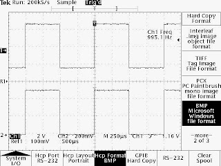
        Data printout

        Not surprisingly, getting this logic analyzer to print its screenshot or memory contents is a challenge nowadays, as the only supported printing method is via an Epson-compatible printer through a parallel port, which has disappeared from most desktop computers ever since the introduction of USB. To workaround this, I have developed a tool which uses a PIC24 to emulate a parallel port printer and stores the printout onto an SD card. The printout can later be converted to a bitmap image (.BMP) by using a Windows program.

        This is the completed tool when assembled on a stripboard using a ST7735 LCD to display output messages:


        See this article for the full source code and other details about the tool.

        Most of the screenshots from the logic analyzer in this article were captured using this tool. The same tool can also be used to capture the device memory contents by pressing the D key while in the Printer Port menu. The output looks like below:

        Memory  | Range is 0000 to 1023 | Timebase 1 | sync  10 uS

        Loc GPA
        bin

        0000 10001000
        0001 10001000
        0002 01110111
        0003 01110111
        0004 01110111
        0005 01110111
        0006 10001000

        The 1230 prints its screenshots as graphics but prints its memory as text. In text mode, Epson escape codes are used to support simple text formatting (e.g. bold). The Windows software I developed can only convert the graphics output to a BMP file. For the memory printout, you can simply read the output file directly using any text editor - most will remove the escape codes (ASCII code < 32) automatically.

        Composite video output

        There is a BNC socket, marked as "Video Out", at the back of the logic analyzer. To test the video output, I salvaged a BNC connector from an old oscilloscope probe and made a BNC to RCA adapter:


        This is the video signal shown on my oscilloscope:

        <

        The signal clearly resembles a monochrome composite PAL signal, albeit with a high peak-to-peak voltage (2.5V). It displays well on my old CRT TV:


        And on my 21" LCD monitor, with the help of a composite-to-VGA converter:


        There are some distortions in the video display, with the bottom and top of the display cut off. This may be due to noises in the video cable or limitations of the video output capabilities.

        Probe teardown

        After testing the overall functionality of the logic analyzer, I decided to perform a teardown of the probe to see its internal components. This is the front and the back of the probe's circuit board:


        Apart from some Tek proprietary components such as TEK 165 2304 01, there are also quite a few 74-series ICs and some MC10H350P PECL to TTL translators. Except for the processing unit in the center of the board, no other ICs are socketed, making it hard to repair if there are issues.

        Other information

        The only useful information I found of this logic analyzer on the Internet is from an old brochure, downloadable from here. It contains basic technical specifications of the 1230 and some information on the different types of supported add-on cards.

        The following Youtube videos, probably converted from the original VHS training tapes made by Tektronix, are also useful:
        Tektronix 1230 training (part 1)
        Tektronix 1230 training (part 2)

        See also my previous article on emulating a parallel port printer to capture the print output from this logic analyzer (and other similar equipments):
        Capturing data from a Tektronix 1230 logic analyzer by emulating a parallel port printer

        Fixing 'Search fields undefined' error when generating source code for a Scriptcase grid view

        $
        0
        0
        When using Scriptcase to quickly develop a web portal in PHP for administrators to perform CRUD (create/read/update/delete) operations on more than 20 tables in an existing database, I encountered the following error during source code generation for a Scriptcase grid:


        The error occurred after I made some adjustments to the grid SQL query while switching between various options in the grid settings and tried to regenerate the code. The details of the error (Search fields undefined) were not shown until I clicked on the folder icon to the right of the Status: Error text.

        Suspecting some SQL query issues, I checked the grid settings but the correct SQL query was entered in Grid>SQL menu:


        The Search module of the grid was also enabled inside the Grid Modules settings. [The error message would disappear and the code generation would succeed if the Search module was disabled for the grid - however, no search capability would be available in this case]


        In other words, there seemed to be no problems with the grid.

        So what is the issue? A Google search on the error message returned this thread as the only result containing a hint The solution: grid_customers...Left:Search...Fields Positioning...middle:the 'valami' push right !!!. This was unfortunately too vague. Or perhaps it was meant for an older version of Scriptcase. Where exactly is the Fields Positioning option and what was the cause of the error message in the first place?

        After several more hours of trial and errors I found the solution. Apparently for every Scriptcase grid, several sets of fields to be shown in list view mode (from the Grid > Edit Fields menu), in record detail view mode (from the Grid > Details > Setting menu), and in search mode (from the Search > Advanced Search/Quick Search/Dynamic Search > Select Fields menu) need to be defined. Although these fields are usually auto-generated, a quick check revealed that the search field configuration for this grid was indeed empty:


        I added the search fields by pressing the >> button to configure all the existing fields for searching:
        The code generation was now successful:
        So the solution is to simply go to the grid search settings and re-configure the fields to be searched. Another few hours of my development time has just been wasted on a trivial issue ....

        But why would the search field list suddenly become empty for this grid? I guess it is because Scriptcase always tries to re-populate the display/search fields in the grid settings when the SQL query changes. Once errors are detected in the SQL query, the display fields will not be populated and will be filled with some default values while the search field list will be emptied. If these errors are later corrected, the display fields will be populated again with the correct entries but the search field list still remains empty, causing the error Search fields undefined. This may or may not be Scriptcase bug, but in any case, the error message is not helpful at all here.

        This is just one of the many scenarios where I wasted my time on understanding certain behaviour of Scriptcase, or trying to locate certain settings. Although I have to agree that Scriptcase has increased my PHP development efficiency by orders of magnitude, the lack of documentation and other usability issues still frustrate me at times.

        I would like to end this post with an announcement for frequent readers of my blog. MD's Technical Sharing is now also known as The Tough Developer's Blog, available at the dedicated domain name toughdev.com. This is in preparation for more exciting changes ahead. Stay tuned for my upcoming articles with more useful tips, tricks and knowledge sharing!

        Error 'Your layout should make use of the available space on tablets' when uploading APK to Google Play

        $
        0
        0
        Recently I received feedback from some customers stating they could not find my application on  Google Play when searching from their Android tablets. The app, however, could be found on Google Play if searched from an Android phone. Interestingly, the APK that was used to upload the same application to Google Play could install and run on the customers' tablets without issues.

        I logged on to my Google Play developer console and immediately noticed an advisory in the screenshot section of the application:

        Your APK does not seem to be designed for tablets

        This is in spite of the fact that I have already uploaded tablet screenshots taken from another tablet for the app entry on Google Play. However, it turned out that simply uploading tablet screenshots is not enough as Google has a set of guidelines, available here, that developers should follow to make their application tablet-ready.

        For those rushing to make their application available to tablet users from Google Play, the bad news is that it is not just a simple tweak on the developer console. You would actually need to modify AndroidManifest.xml to indicate tablet compatibilities and reupload the APK. The good news is that not all 12 criteria listed by Google on the Tablet App Quality are actually required for the app to show up on Google Play as a tablet app. In fact, during my testing, only the following are needed, at a minimum:

        • Target Android Versions Properly - by setting correct values for targetSdkVersion and minSdkVersion
        • Declare Hardware Feature Dependencies Properly - by setting appropriate values for uses-feature and uses-permission elements
        • Declare Support for Tablet Screens - by setting correct values for supports-screens element
        • Showcase Your Tablet UI in Google Play - simply by uploading at least two tablet screenshots, one for 7-inch devices and one for 10-inch devices

         With the above changes, the error message when uploading my APK now changed to:

        Your layout should make use of the available space on 7-inch tablets 
        Your layout should make use of the available space on 10-inch tablets

        Unfortunately Google Play did not provide much useful information for these errors: 


        A search on Google for these errors returned no conclusive results. Some replies suspected that Google Play analyzes the APK looking for design elements specific to tablets (e.g. looking for layout folder with names layout-sw600dp, layout-sw600dp-land, layout-sw720dp, layout-sw720dp-lan, etc. or looking for an XML layout with large screen width) while others say that Google Play is simply analyzing the screenshots I uploaded to see if it looked like a tablet app, not a phone app running on tablet with huge unused white space lying around.

        Well, if it's indeed analyzing the screenshot, is there a way to make it think that my screenshots are tablet-compliant? The answer is, surprisingly, to use the Device Art Generator from Google itself and drag your phone app screenshot to the tool, selecting the Nexus 9 which has tablet resolution:


        This is the generated image, with the device skin overlayed on top of the original screenshot from a simple Hello World application:

        Surprisingly, Google Play accepted this screenshot as tablet-compliant and finally decided to make my app available on tablets!

        So I guess the conclusion is that Google simply analyzes the tablet screenshots and looks for white space, most likely from the bottom and perhaps from the right and complains that the app is not tablet-compliant if there is too much white space. This assumes that a properly designed tablet app should make full use of the screen space and expand all the way to the bottom of the screen. By using the Device Art Generator, we have satisfied this criteria by adding the device skin around the screenshot and make Google think that screen space is fully utilized!

        While I do not support anyone using this trick on production apps, the Device Art Generator tool is good as a quick fix for developers to make their existing phone-only apps on Google Play available on tablets without the hassle of re-designing the existing app layout files.

        Keyboard issues in GRUB bootloader on a Mac Mini booting Mac OS, Windows and Ubuntu Linux

        $
        0
        0
        The Mac Mini, my main machine for daily work, has the following partition configuration for triple-booting Windows, Mac and Ubuntu Linux: 
        • Partition 1: Mac OS X (HFS+)
        • Partition 2: Windows 8 (NTFS)
        • Partition 3: Ubuntu Linux (Ext4) 
        • Partition 4: DATA (NTFS)
        rEFIt is used as the boot manager to allow me to select which partition to boot from at startup. GRUB2 is installed on partition #2 and configured to select between Windows 8 and Linux. This configuration has been working well for a few years.

        However, recently after the old USB keyboard (a Microsoft Wired Keyboard 600) failed and had to be replaced with a Prolink PKCS-1002 keyboard, I could no longer select between Windows and Linux at the GRUB2 boot menu, and the system booted to Windows by default. The selection of the Mac OS X partition from the rEFIt menu still worked fine. Once booted to Mac OS, Windows or Linux (by changing the GRUB default entry), I could use the keyboard without hassle. The keyboard issue would still remain even when the Windows 7 BCD bootloader was used, suggesting that the issue was not specific to the GRUB bootloader.

        You would probably tell me to go to BIOS and enable USB legacy support, but hey, this is a Mac that uses EFI and boots Windows via BIOS emulation, which most likely would already have legacy USB support, otherwise the old keyboard could not have worked.

        Adding keyboard support to GRUB menu

        After some research, I decided to follow the advice in this forum thread, which basically told me to add the following lines to /etc/default/grub:

        GRUB_PRELOAD_MODULES="usb usb_keyboard ehci ohci uhci"
        GRUB_TERMINAL_INPUT="usb_keyboard"


        and run:

        grub-mkconfig -o /boot/grub/grub.cfg
        update-grub2

        Well, I tried that and turned out to be a big mistake. The USB keyboard now indeed worked fine in the GRUB menu but selecting any entry would only return error grub error: disk (hd0,msdos5) not found. A simple ls in the GRUB rescue console resulted in the same error. I guess the preloading of keyboard modules at the GRUB menu disrupted the initialization of other system driver packages and the system failed to recognize the hard disk partition to boot from.

        I stupidly did not backup my grub.cfg file and the only recourse was to boot from a Ubuntu Live CD, revert the above change to /etc/default/grub and follow this guide to restore the GRUB default configuration. Fortunately this worked and I was back to square one, with a non-working keyboard at GRUB menu.

        Keyboard compatibilities

        At this point I decided to buy another keyboard, a Logitech K120, and see if the same issues still persist. Surprisingly everything worked and I was able to use the new keyboard to select either Windows or Linux to boot to.

        So what is the issue causing only the Prolink keyboard not to work? I checked the hardware ID of all three keyboards from Windows Device Manager:

        Logitech K120: VID_046D&PID_C31C [working at GRUB menu]
        Microsoft Wire Keyboard 600: VID_045E&PID_0750  [working at GRUB menu]
        Prolink PKCS-1002: VID_1A2C&PID_0027 [not working at GRUB menu]

        All 3 keyboards are recognized as HID Keyboard Device by Windows:


        Despite much effort, I could not find anything from the Device Properties page of the Prolink keyboard that could provide any hint why it could not work. I can only hazard a guess that its implementation of USB Human Interface Device is flawed causing it to fail to work with the emulated BIOS at the GRUB menu while Windows, which presumably has more sophisticated error handling, is able to detect the keyboard without issues.

        IPDGen - Blackberry IPD backup generator from SMS CSV files

        $
        0
        0
        In view of the popularity of CSV2IPD, a utility which I developed back in 2010 that reads text messages from CSV files and generates an IPD file that can be imported to Blackberry devices, I have decided to put in some efforts to to further improve CSV2IPD and release its next version, known as IPDGen- short for IPD Generator.

        Similar to CSV2IPD, IPDGen also accepts CSV files as input and will generate an IPD file containing the text messages. It however has the ability to auto-detect the CSV file format and identify the columns containing the message text, phone number and timestamp, thus reducing the need to manually format the CSV files, making it easier to use.

        IPDGen will require .NET Framework 3.5 to run properly. The framework will be automatically installed on Windows 7 and above if it is not already installed. If you are using Windows XP, you can download it here.

        This is the main user interface of IPDGen:


        Improvements

        The following features have been implemented:
        1. Option to indicate whether incoming and outgoing text messages are in a single file, or multiple files.
        2. Options to configure various CSV settings such as delimiter character, offset row and text encoding
        3. Options to specify columns storing the message properties
        With IPDGen, you can just click Browse to select the CSV files, and click Detect Settings to have it detect the CSV format for you:


        The message text, phone number and timestamp columns can be detected automatically as seen from the above the screenshot. You can then just click Convert to save the messages to an IPD file. Once done, IPDGen will report the results:


        You can now preview the generated IPD file to check if the messages have been processed correctly. This is a major improvement from CSV2IPD where only the total number of imported messages is reported.

        More information

        You can find out more information on IPDGen at:

        IPDGen home page
        Support forum
        Knowledge base

        Unfortunately due to development costs, IPDGen is not free. A trial version, which can convert up to 25 messsages, can be downloaded for users who want to experiment with the application features. You should purchase a license in order to fully convert your text messages.

        The original version, CSV2IPD, will remain free and continues to be supported for those who do not need the advanced features of IPDGen.
        Viewing all 63 articles
        Browse latest View live